

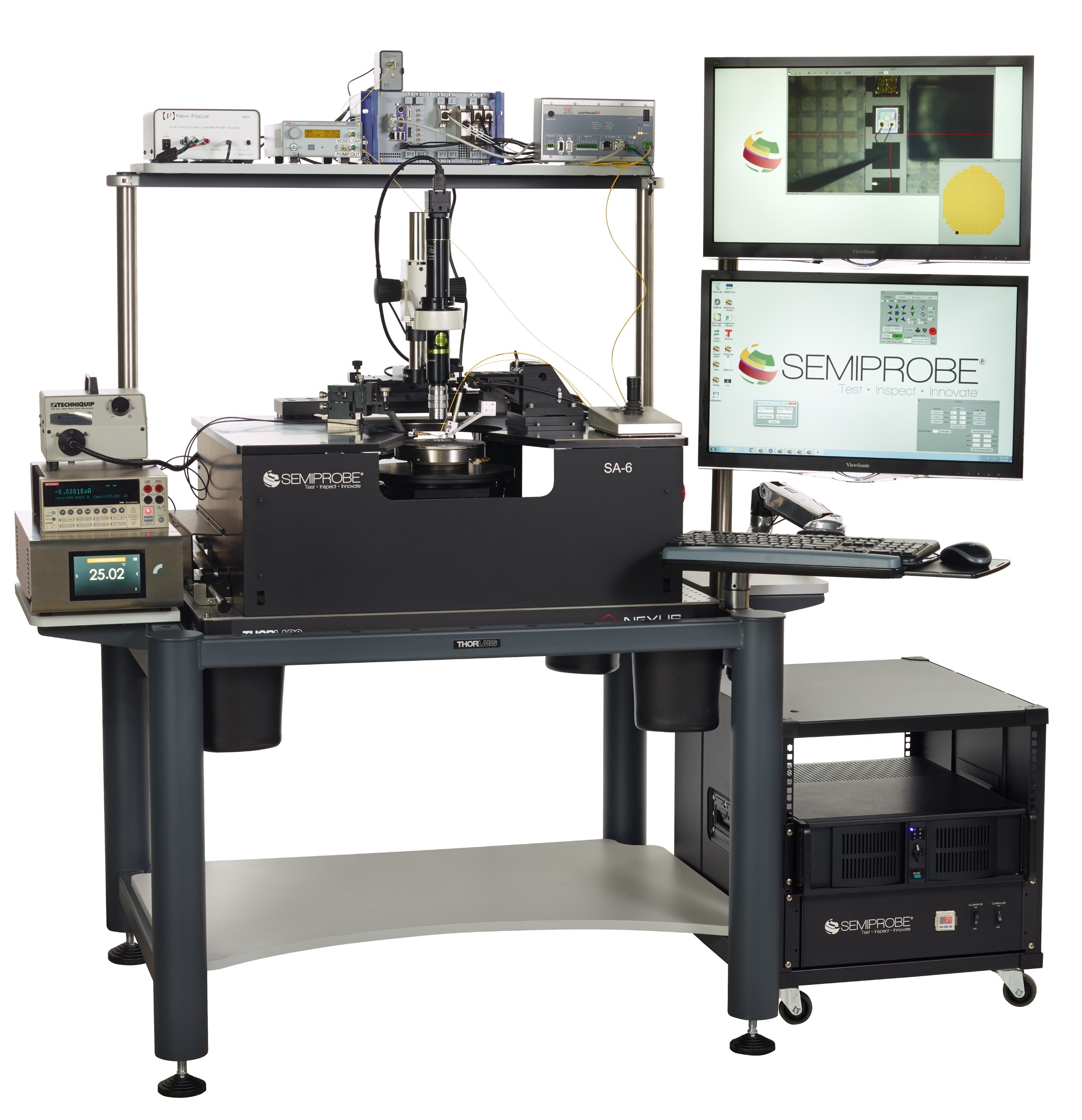
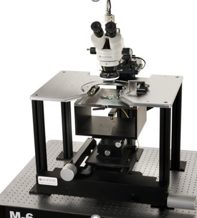
The customer wanted a 150 mm semiautomatic probe system to test vertical cavity surface-emitting laser diodes (VCSELS). The VCSELS were in wafer and individual die form and tested at temperatures ranging from 25 C to 200 C. The customer required the device to be biased from the top and bottom. A manual manipulator with a multi-contact DC wedge was used for biasing. A second manual manipulator was used for a non-contact height measurement sensor. An optical fiber was required to collect the light and it needed to be mounted to a three-axis programmable manipulator with a goniometer.
'To learn more about this Wafer Prober Click Here
The customer wanted a turn-key probing and testing system to test optoelectronic devices. They needed to test whole wafers, partial wafers and individual die. They needed a semiautomatic probe system that had double-sided probing (DSP) capabilities. The device would be stimulated from the top with a probe card or individual manipulators and the backside would have a detector mounted on a programmable X,Y and Z stage to collect the light output. The environment had to be dark and the devices needed to be tested at temperatures ranging from ambient to 225 C. The customized graphical user interface (GUI) had to control the prober and test instrumentation as well as collect the data.
To learn more about this Wafer Prober Click Here
Using a semiautomatic 150 mm probe system the customer wanted to test light emitting diodes (LEDS) in wafer form, on 150 mm and 200 mm metal frames and plastic rings. The wafers needed to be tested from ambient to 200 C using a thermal chuck. The LED device would be tested using probe cards and stimulated from the top and bottom. The light output would be captured by an integrating sphere (cube) mounted on multi-axis pneumatically controlled stages that allowed the integrating sphere to moved in and out of position and up and out of the way for changeovers. Customized fixturing to address all of the requirements was required.
To learn more about this Wafer Prober Click Here
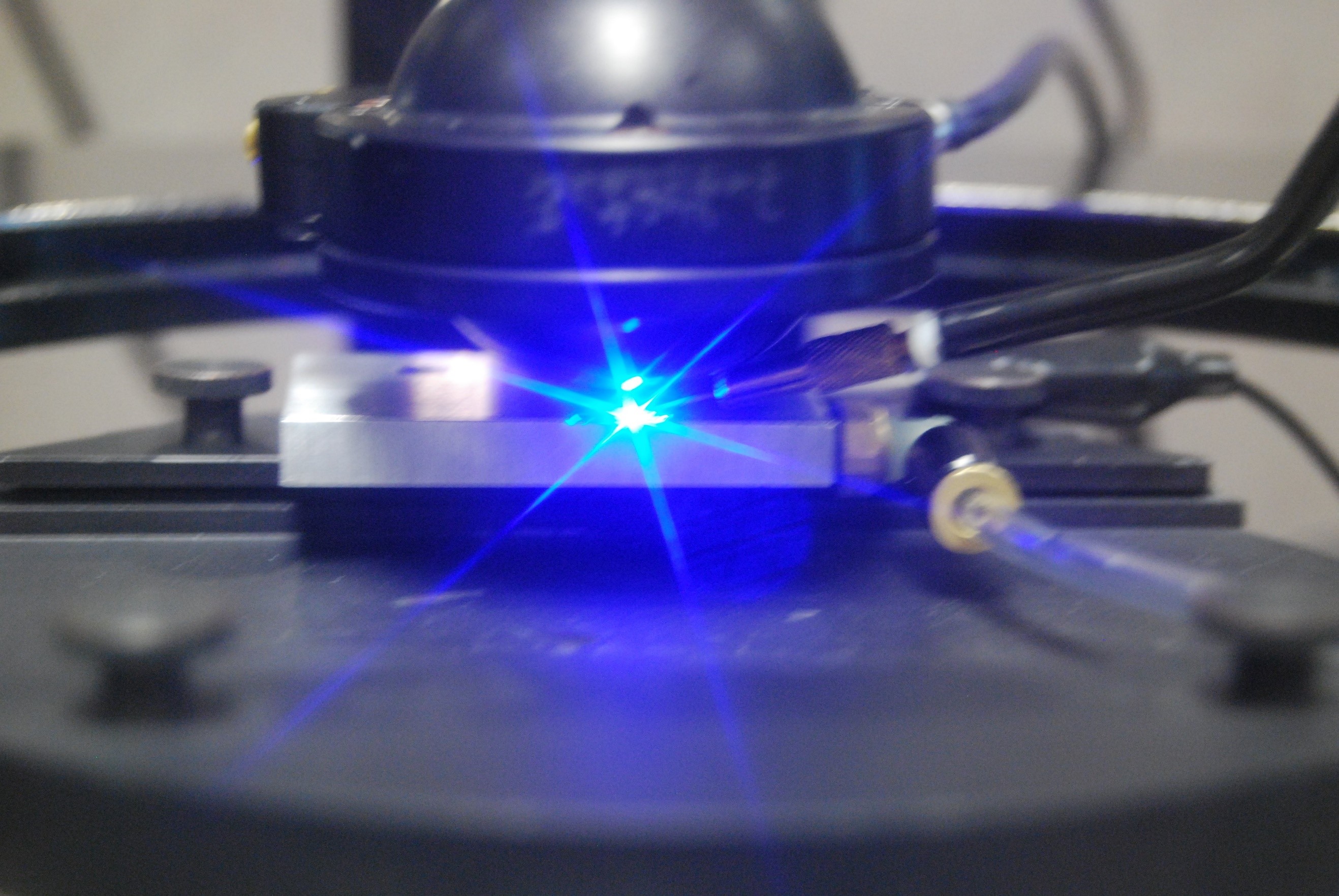
The customer wanted a multipurpose semiautomatic probe system to test vertical-cavity surface-emitting laser diodes (VCSELS) and edge-emitting laser diodes (EELDS) on the same system using a single integrating sphere. The VCSELS would be in wafer form and the EELDS would be in laser bars.
To learn more about this Wafer Prober Click Here
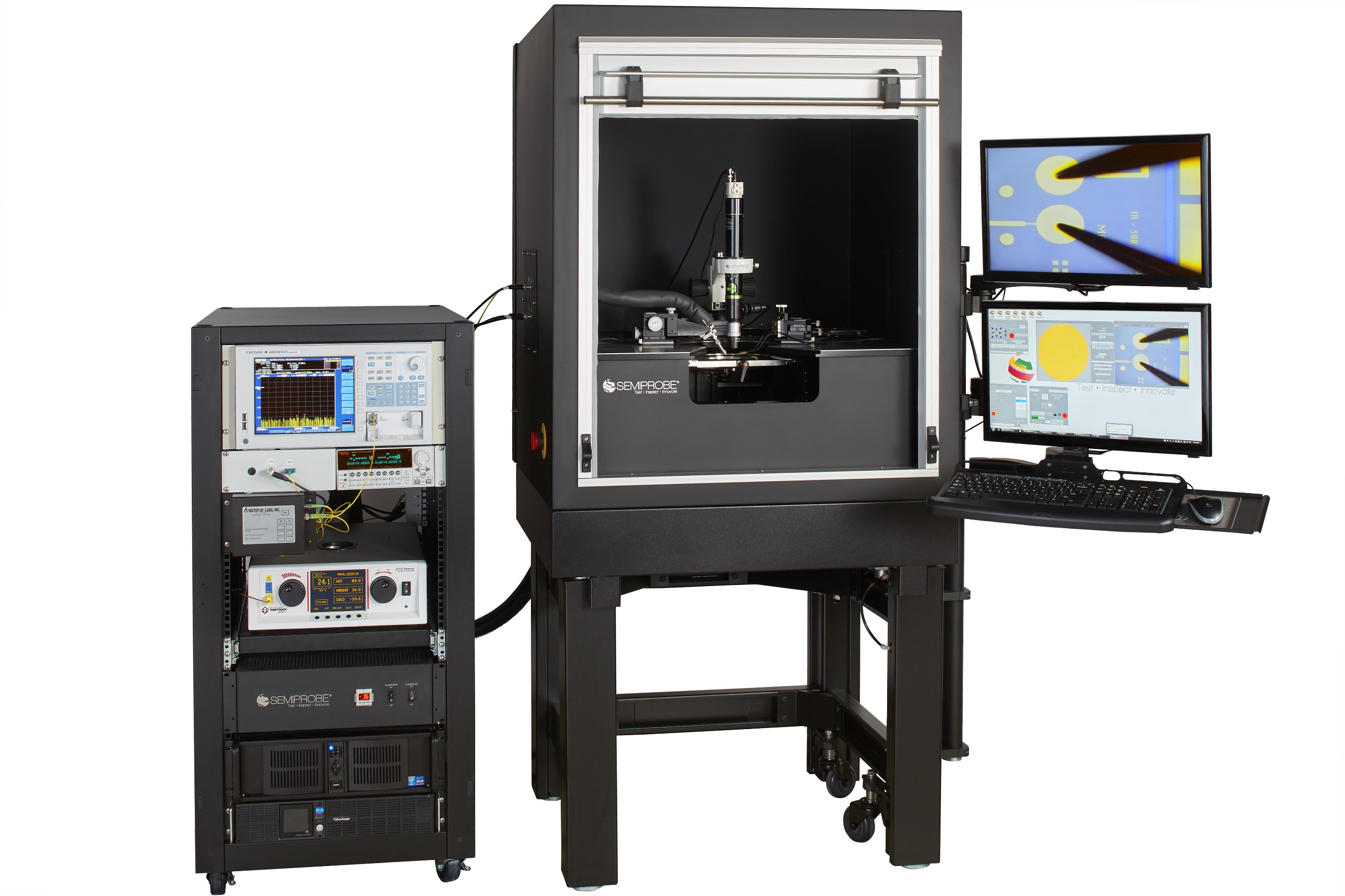
The customer wanted a manual double-sided probing (DSP) system to test silicon photonic chips and wafers using probe cards and manipulators. The top side of the device would be biased and the backside of the device had a light output that was captured by a detector. The detector was mounted on a manual X,Y, Z and theta stage. The devices tested had a variety of dimensions so a universal mechanically clamping chip carrier was designed to hold the devices. Carriers for different size wafers were also required.
To learn more about this Wafer Prober Click Here
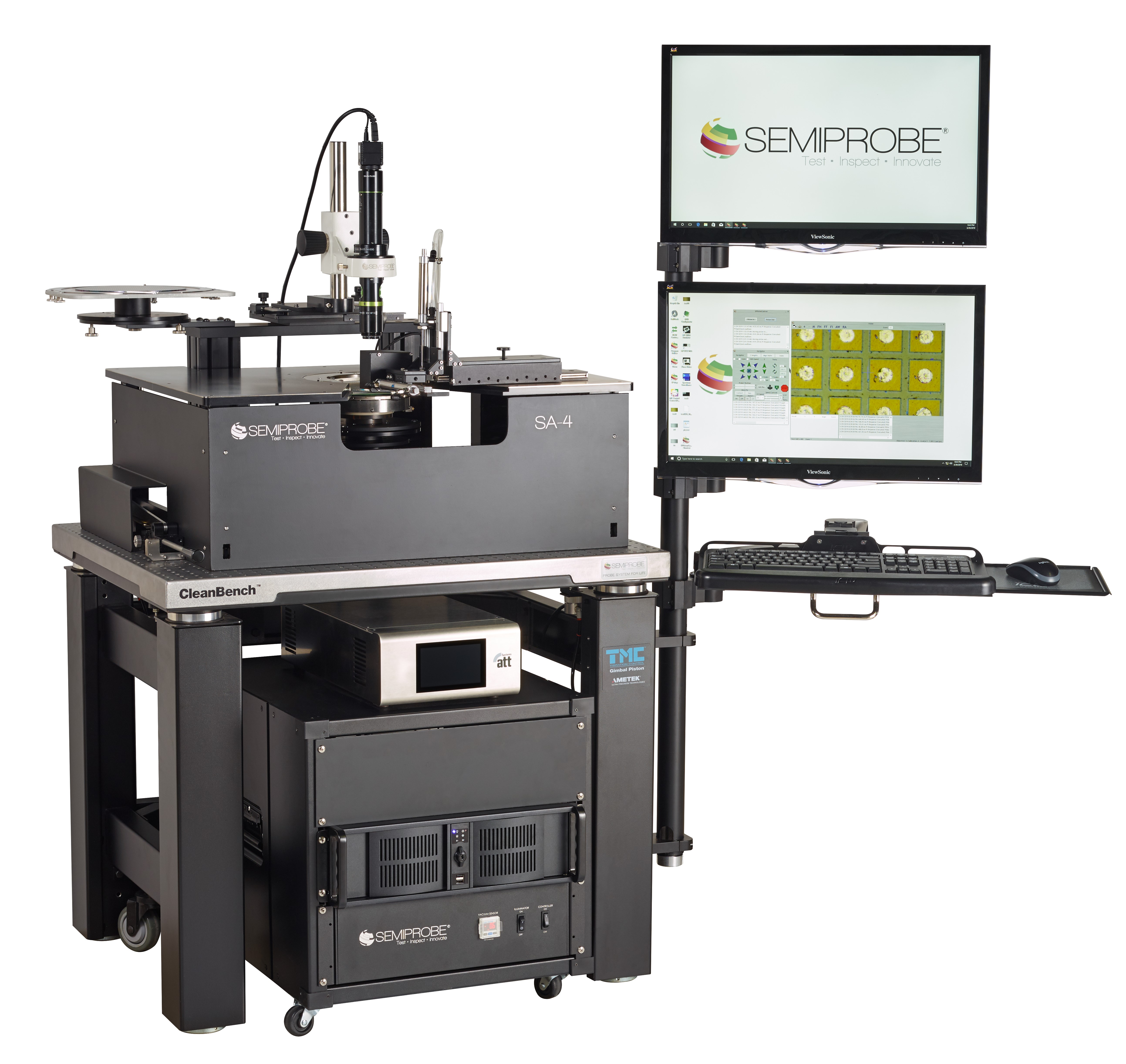
The customer wanted a semiautomatic probe system to test light emitting diodes (LEDS) in a few different modes - wafer form, wafers sawn and stretched on frames or rings, as partial wafers and as individual die. The device would be biased with a DC manipulator and the light output would be captured by an integrating sphere. The integrating sphere needed to be moved in and out of position on a repeatable basis when required.
To learn more about this Wafer Prober Click Here
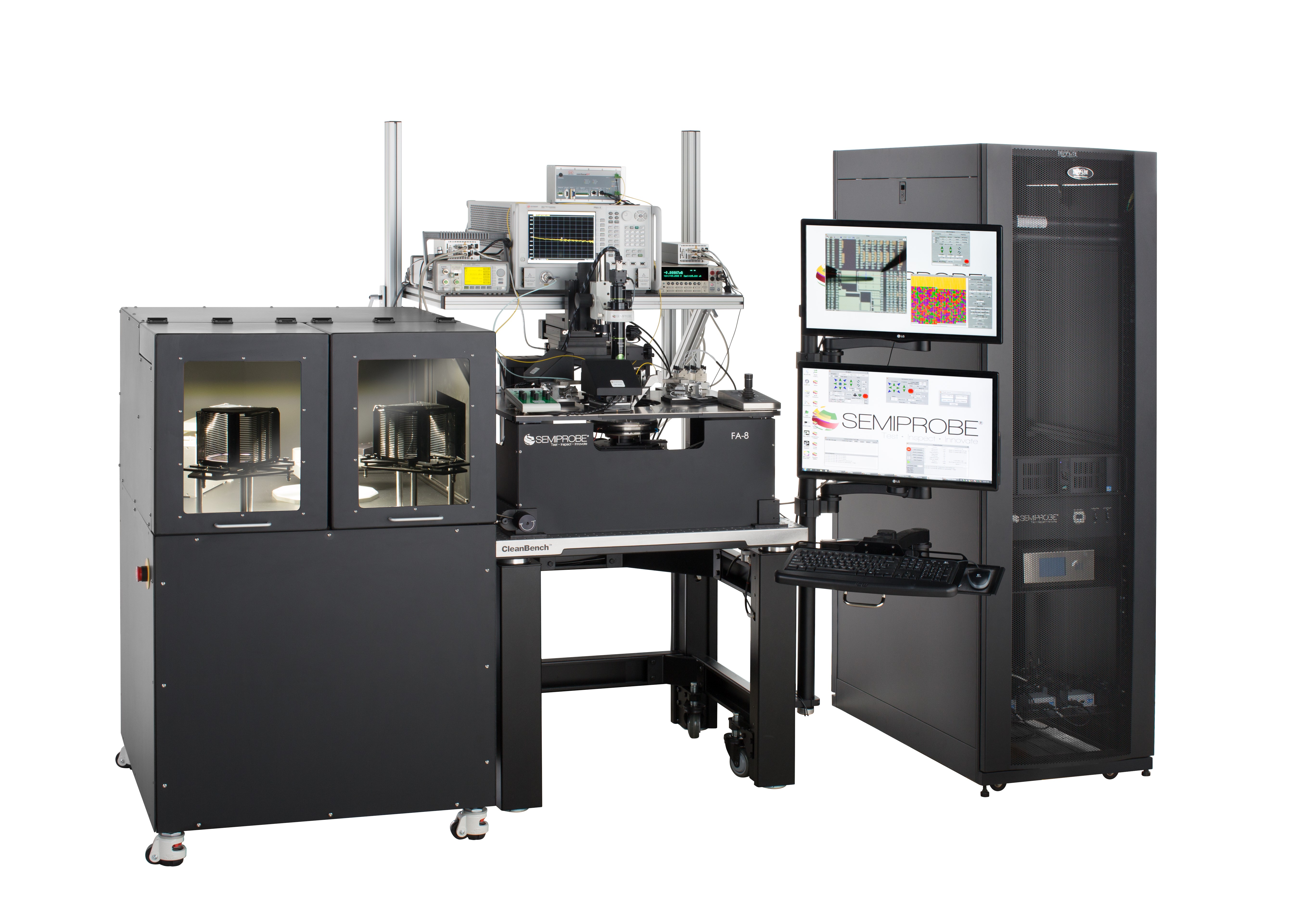
The customer wanted a 300 mm fully automatic double-sided probe system for high volume silicon photonics testing in a production environment. The system had to provide the ability to bias the device with a probe card on the top while detecting light output from the bottom of the wafer. The system needed to provide low and high temperature capability from -40 C to 200 C in a frost-free and shielded environment. The system had to be able to operate 24 hours a day, 7 days a week. The system had to be tested to and certified to a variety of SEMI, UL and other safety standards.
To learn more about this Wafer Prober Click Here
The customer wanted a fully automatic probe system to test silicon photonic devices in wafer form that were manufactured using MEMS technology. Due to small pitches and tight tolerances the customer needed four (4) programmable manipulators. Two (2) manipulators were multi-axis hexapods and two (2) were three-axis manipulators. The two hexapod manipulators had probe arms that could handle single and multi-mode fibers. The fiber needed to be placed within 10 um of the device surface so non-contact height measurement sensors were required and mounted to the fiber arms. The two (2) three-axis manipulators used single DC or High Frequency (HF) probe arms with the appropriate probe tips.
To learn more about this Wafer Prober Click Here