Customer Requirements:
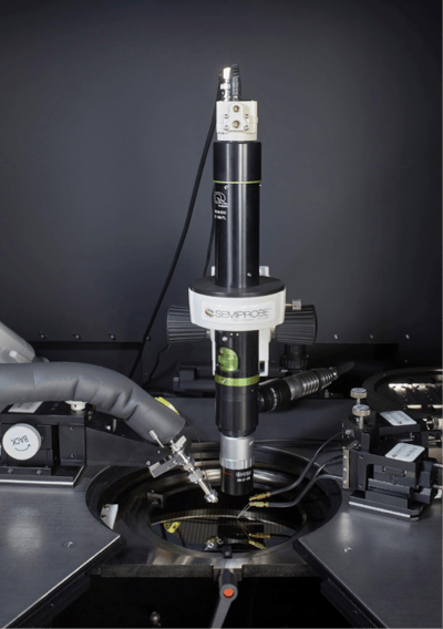
The customer wanted a turn-key probing and testing system to test optoelectronic devices. They needed to test whole wafers, partial wafers and individual die. They needed a semiautomatic probe system that had double-sided probing (DSP) capabilities. The device would be stimulated from the top with a probe card or individual manipulators and the backside would have a detector mounted on a programmable X,Y and Z stage to collect the light output. The environment had to be dark and the devices needed to be tested at temperatures ranging from ambient to 225 C. The customized graphical user interface (GUI) had to control the prober and test instrumentation as well as collect the data.
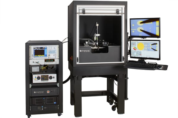 Double-sided Optoelectronics Semiautomatic Wafer Prober
Thermal Wand
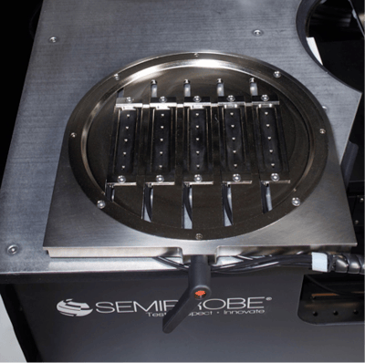
Individual Die Carrier
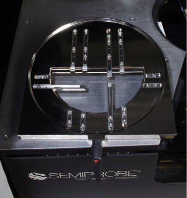
Partial Wafer Carrier
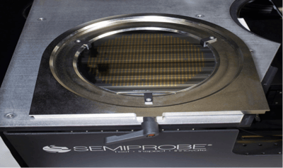
Wafer Carrier
Solution:
- Turn-Key Double-Sided Probing (DSP) System with Test Instrumentation
- Semiautomatic 200 mm Probe System 200 mm programmable X,Y,Z and theta stage
- PILOT Software Suite – Navigator, Wafer Map and Autoalign
- Customized Graphical User Interface (GUI)
- Top side probing with manipulators or probe card and bottom side light detection with detector
- Carriers for wafers, partial wafers and individual die
- Thermal System – ambient to 225 C
- Programmable coarse and fine stage for optical detector
- Dark Box, interconnect panels and a Vibration Isolation Table
To learn more about other Advanced Optoelectronic Wafer Probers Click Here.