Customer Requirements:
- The customer wanted a small footprint, a multi-purpose probing system configured with DC and HF frequency manipulators that could probe devices up to 110 GHz. The system needed to be compact to allow them to ship to multiple users in Canada. Manipulators with frequency extender mounts needed to be designed to mechanically clamp to SemiProbe as well as competitive probe system platens.
SemiProbe High-Frequency Wafer Probe Station Solution:
Key System Components:
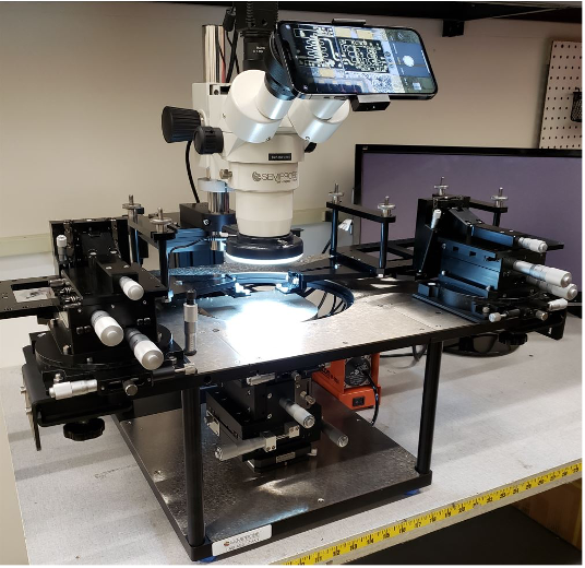
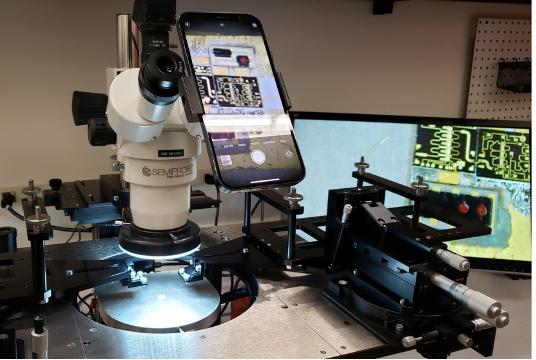
- LA-100 HF manual probe system consisting of:
- Manual Wafer Stage with coarse and fine movement
- 100 mm HF chuck with two (2) independent calibration substrate holders
- Large Platen with removable front wedge – stainless steel skin for magnetic-based manipulators
- Microscope Post with Microscope Movement – coaxial – X & Y travel of 100 mm x 100 mm
- Cell Phone Adapter – universal – used to see and capture images with and without a monitor
- Two (2) MA-8500 manual manipulators with clamping bases and universal frequency extender modules. Clamping bases are designed to fit on most probe system platens.
- Vacuum Pump – small footprint and quiet

Topics:
Application - High Frequency,
Success Stories
Denis Place is one of the founders of SemiProbe and has more than 35 years of experience working in the international semiconductor industry. He has degrees in electrical engineering and business management. Place is in a unique position, because he personally used and worked with probing systems for many years before starting his own semiconductor probing company.

