High-Frequency Wafer Prober Customer Requirements:
- Customer was looking for a general-purpose 200 mm manual high-frequency wafer probe system that allowed for the measurement of individual parts mounted on tape as well as whole wafers up to 200 mm over a variety of frequency ranges. They wanted to use individual manual manipulators with standard West/East high-frequency probe arms that could handle GS, SG, GSG, differential, and multi-contact wedges that operated from DC to 40 GHz. In addition, they wanted the ability to add some manual manipulators to be used for DC bias and a probe card holder for probe cards.
SemiProbe High-Frequency Wafer Prober Solution:
Key High-Frequency Wafer Probe System Components:
- Rapid Align manual wafer stage that provides coarse and fine stage travel, 200 mm high-frequency chuck with vacuum holes and two (2) auxiliary chucks for calibration substrates, linear platen lift with coarse and fine platen lift, large platen with removable front wedge, and stainless steel skin, microscope post with 100 mm x 100 mm of linear X,Y microscope movement, stereo zoom microscope with a long working distance and field of view, a CCTV system, a rotating monitor stand, two (2) complete MA-9100 manual manipulators with West/East high-frequency arms and magnetic bases, two (2) complete MA-9000 manual manipulators with adjustable probe arm faceplate, coaxial arms and magnetic bases, a 4.5” wide probe cardholder and a variety of tungsten probe tips for DC bias, high-frequency probe tips and calibration substrates from GGB Industries, and Junkosha high-frequency cables.
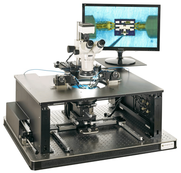 Manual 200 mm High-Frequency Wafer Prober with manual HF manipulators and GGB Model 40A GSG probes
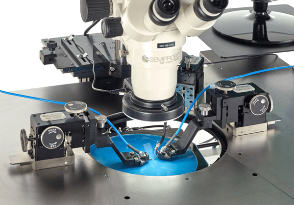 High-Frequency Wafer Probing on stretch frame with MA-9100 manual manipulators with West/East probe arms, GGB Model 40A GSG probes, Junkosha HF cables, and an MA-9000 with coaxial probe arm for DC bias
 High-Frequency probe card with probe card holder
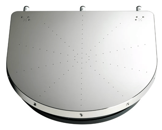
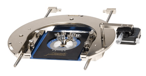
200 mm High-Frequency vacuum chuck with vacuum holes and independent auxiliary chucks for calibration substrates