High Frequency Wafer Prober Application - Customer Requirements:
- The customer wanted a modular manual probe system to characterize 150 mm and 200 mm wafers and packaged parts up to 750 GHz using Virginia Diode WR 1.5 Frequency Extender
SemiProbe Solution:
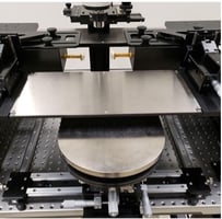
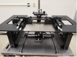
SemiProbe Probe System for Life (PS4L) M-8 manual probing system configured with Virginia Diode Frequency Extenders for testing High-Frequency devices up to 750 GHz
Key System Components:
- Probe System for Life PS4L M-8 HF manual probe system consisting of:
- Vibration Isolation Table (VIT) with casters and leveling feet
- Rapid Align manual wafer stage
- 200 mm high-frequency chuck with two (2) independent calibration substrate holders
- Large Platen with stainless steel skin for magnetic-based DC manipulators – up to four (4)
- Microscope Post with microscope movement – coaxial and linear 100 mm X & Y travel
- Fusion Zoom Tube Compound Optics with long working distance objective
- CCTV System – color camera, 24” color monitor, and monitor stand
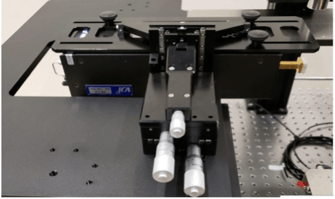
- Two (2) MA-8500 manual manipulators with universal extender module mount customized for the VDI Frequency Extender Heads, Formfactor, and GGB Industry probes
- Two (2) MA-9000 manipulators with coaxial probe arms used for DC bias
- Vacuum and Pressure Pumps
Customer Testimonial: "The prober exceeded our expectations -- once installed, we were easily and painlessly probing several different devices. We've found the SemiProbe system really easy to use. We plan to upgrade it as our test needs grow. You'll be the first folks we call when we expand our station capacity in the future”