Customer Requirements:
VentureLAB, a Canadian company located in Markham ON, started a new Hardware Initiative Lab to provide multiple measurement capabilities to Canadian companies, start-ups to large companies. They wanted a semiautomatic probe system that allowed them to easily configure it to meet a variety of device characterization capabilities for testing die, partial wafers, whole wafers, and packaged parts at temperatures ranging from -65 C to 200 C.

SemiProbe High-Frequency Wafer Prober Solution for VentureLAB:
Key System Components:
- Probe System for Life PS4L SA-8 HF semiautomatic probe system consisting of: o Vibration Isolation Table (VIT) with casters and leveling feet
- 200 mm Programmable X,Y,Z, and theta stage with control electronics
- Load Stroke – for easy device loading and unloading
- 200 mm thermal chuck system with triaxial addon surface and independent HF auxiliary chucks (2) that operates from -65 C to 200 C
- Large Platen with stainless steel skin for magnetic-based manipulators, removable front wedge, and linear platen lift (coarse and fine)
- Manipulators – four (4) manual MA-9000 with West/East and North/South HF, coaxial and triaxial probe arms
- Adjustable Package Part Holder – includes mounting plate for the thermal chuck
- Probe Card Holder
- Localized Environmental Chamber (LEC) – with top-hat and LEC cover plate, provides a light tight, EMI, and frost-free environment
- Microscope Post with microscope movement – coaxial and linear 100 mm X & Y travel
- Fusion Zoom Tube Compound Optics with long working distance objectives
- CCTV System – color camera, 24” color monitor and monitor stand
- PC/Monitor/GPIB/Adjustable Monitor/Keyboard/Mouse Rack
- PILOT Software Suite – Navigator, Wafer Map and Auto Align
- Two (2) customized tuner mounts for Focus Microwave Multi-Purpose Tuners, model MPT-1818 that operate from 1.8 GHz to 18 GHz
- Vacuum and Pressure Pumps – small footprint and quiet
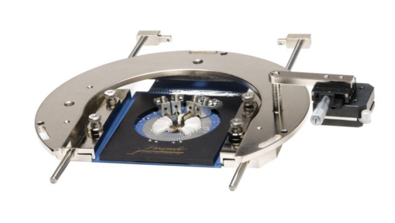 Probe Card Holder with a High Frequency Probe Card used with the SemiProbe Semiautomatic SA-8 HF Wafer Prober...
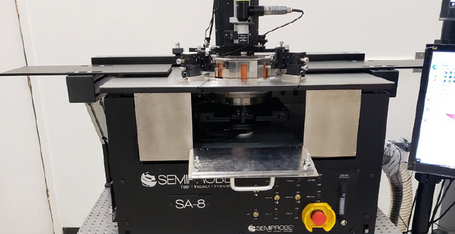
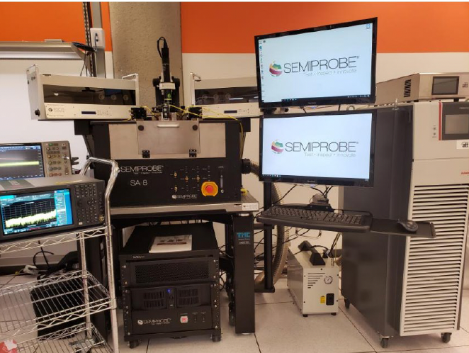 SemiProbe SA-8 HF prober system configured to test high-frequency devices at low and high temperatures
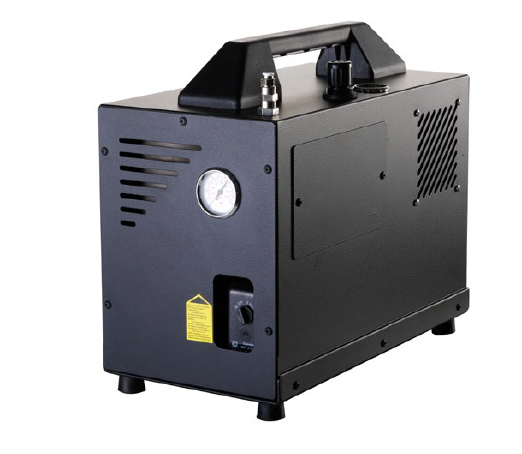
Accessory - small footprint and quiet air compressor
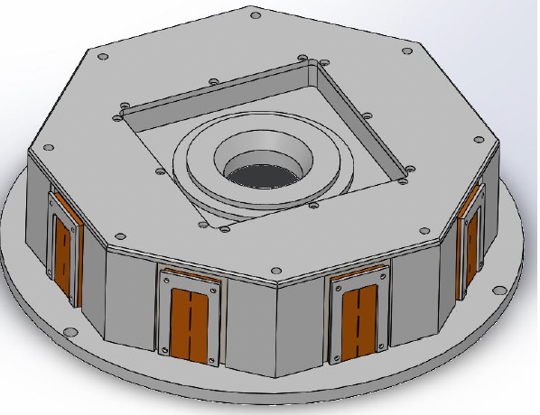
Top Hat used with the Localized Environmental Chamber (LEC) that provides light and EMI shielding in a frost-free environment operating from -65 C to 200 C
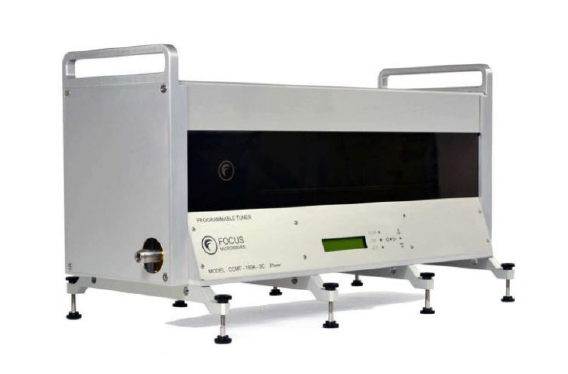 Focus Microwave Multi-Purpose Tuner, Model MPT-1118, interfaced with the SemiProbe SA-8 semiautomatic probe system for High-Frequency measurements
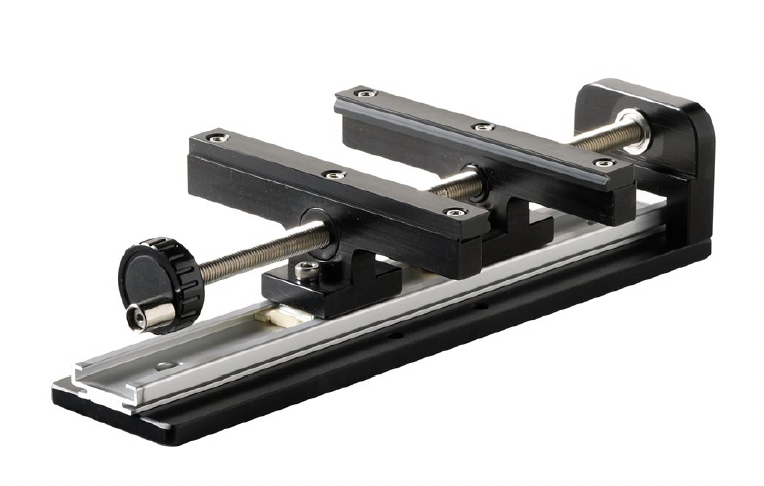
Adjustable Packaged Part Holder
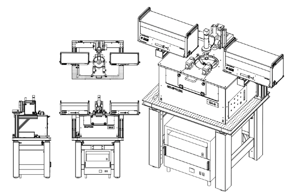
Multiple Views of SemiProbe SA-8 semiautomatic High Frequency wafer prober system configured with the Focus Microwave Multi-Purpose Tuners
SemiProbe SA-8 High-Frequency probe system with a Localized Environmental Chamber for -65C to 200 C temperature testing
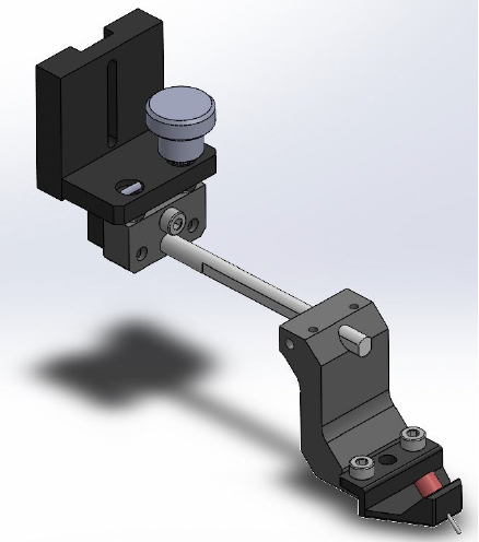
High-Frequency Probe Arm and Probe used with SemiProbe Top Hat and Localized Environmental Chamber