 There are a number of ways to test whole silicon wafers in production. In most cases all die on the wafer are tested and this is often referred to as 100% probe, production, final probe, final test and more. The primary modes of identifying bad die on the wafer is with inking or wafer mapping. If inking is used the die are normally tested to one program (part number) and they are either good or bad. If a die is bad an ink dot is applied to the center of it. The die with ink dots are normally not picked up from the frame (manually or with a pick & place arm) at later processing. A die with an ink dot does not mean the device was a complete failure. It means the device did not meet the electrical requirements of the test program. The most popular method of testing die is with a wafer map program.
 The advantage to wafer mapping is multiple programs and binning can be used. This allows for better wafer utilization because multiple good part numbers can be saved for later use. After 100% probe the wafers are normally sent to be sawn. The sawing process usually involves mounting the wafers on a sticky tape that is affixed to a metal frame or plastic ring (hoop). The sticky side is where the wafer is mounted and it holds the die in place after the wafer has been sawn (all streets in X and Y).
 The die is now in a singulated mode and it is not uncommon for some companies or customers to want to test the die again. The primary reason for re-testing is because saw induced failures can occur and it is possible that some die that were originally electrically good at 100% probe may now be bad after saw (cracks, chip outs, ESD damage could induce electrical failures). Other reasons for testing again is because the die is being mounted into an expensive package or housing that can’t be re-worked or is difficult to re-work. Another is because the parts are being used in a Hi-Rel (high reliability) application (medical, military, satellite and more). In all cases the additional testing increases the average selling price (ASP) of the die due to the additional screening required but still less in comparison to the packaging costs. There are companies, often referred to as die houses, that will purchase whole wafers, partial wafers, wafers mounted on frames and sawn as well as individual die placed in waffle packs or Gel pack containers from wafer foundries
 They add value to their customers with additional electrical testing, visual inspection, documentation and the willingness to sell in small quantities. Die houses, foundries and other companies often provide die that are referred to as Known Good Die or KGD.
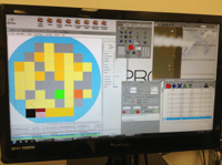
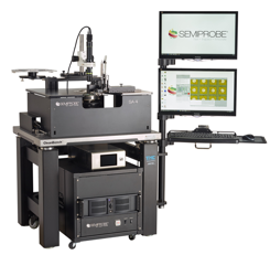
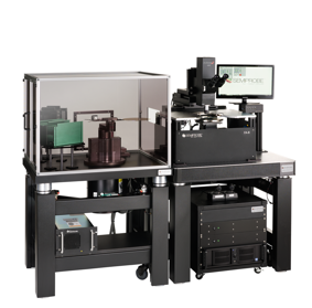
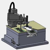
SemiProbe has a family of probe systems – manual, semiautomatic and fully automatic that can test whole wafers, partial wafers, wafers sawn and stretched on frames as well as individual die in trays or mounted on frames. All semiautomatic and fully automatic probe systems have a programmable X,Y,Z and Theta stage and that ability combined with the PILOT Software Suite (Navigator, Wafer Map and Autoalign) provides the ability to test singulated die on frames as well as in trays.
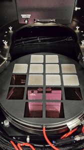
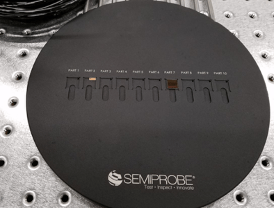
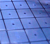
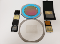 It is not uncommon to build customized trays that are universal in design to hold a few different sized die (chips). In most cases a small vacuum hole is drilled in the bottom of the tray that allows the individual die to be held in place via vacuum when the tray is placed on the standard wafer chuck (ambient or thermal chuck). In some applications vacuum can’t be used so mechanically clamping the individual die is required. The cavity of the tray has to be larger than the die so that means that the chips can vary in X,Y and Theta rotation relative to each other. The probe system, using the capabilities mentioned above, will automatically align each chip prior to testing. Individual manipulators or probe cards can be used. The die results can be saved with a wafer (die) map or inked with an inker.
To provide additional capabilities for Known Good Die (KGD) requirements SemiProbe also provides integrated pick & place arms as well as inspection modules into our patented Probe System for Life (PS4L) platform. With the pick & place arm the user has the ability to test die on a frame or in a tray using the probe system chuck and place the tested device in either a tray, trays or a frame placed on the platen.
In most cases a Known Good Die (KGD) probing solution will be application specific. Most of the system configuration will use standard probe system components with some being customized for the customers application
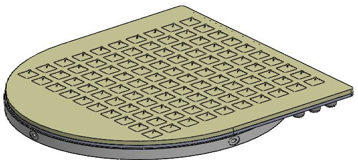
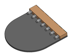
Examples of some customized die (chip) and bar trays: