Customer Requirements:
A semiautomatic probe system is used for production testing of 150 mm and 200 mm MEMS wafers using probe cards, a dispensing system, and a Keithley S500 test system.
SemiProbe MEMS Microfluidics Wafer Probe System Solution:
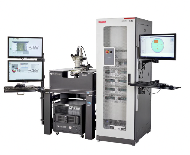
MEMS Microfluidic 200 mm Semiautomatic Probe System with Keithley S-500 Test System
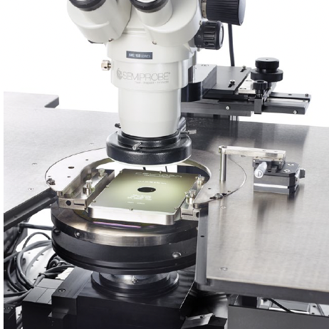 MEMS Semiautomatic Probe System with a Probe Card
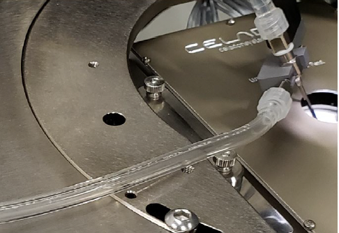 MEMS. Microfluidic Dispense System
Key MEMS Microfluidics Wafer Testing System Components:
- Vibration Isolation Table (VIT) with casters and leveling feet
- A programmable X, Y, Z, and theta stage with control electronics. The wafer stage has > 200 mm of X and Y travel
- 200 mm standard wafer chuck
- Probe Card Holder with coarse and fine theta adjustment
- Microscope Post with linear and coaxial X & Y microscope movement – 100 mm x 100 mm
- Stereo Zoom Microscope – with long working distance of 100 mm
- CCTV Camera System – color camera, 24” color monitor
- PC/Monitor/GPIB Card
- PILOT Software Suite – Navigator, Wafer Map, and Auto Align
- Keithley Test System controlled from the S500 Automated Characterization Suite (ACS) software using the SemiProbe driver via GPIB
- Dispense System – custom-designed – pump with two (2) dispense units
- Test Instrumentation – Keithley S500 Series