SemiProbe provided a turnkey and Integrated 200 mm Semiautomatic MEMS Probe System with an Olympus Metallurgical Microscope for a large Wafer Foundry.
Customer Requirements for their MEMS Wafer Prober System:
- Complete turnkey and integrated MEMS wafer probing system to test up to 200 mm microfluidic MEMS wafers over temperature
- Integrated solution had to provide a fully functional MEMS wafer probing and high magnification inspection capabilities using one platform
- Programmable Manipulators for electrical testing and fluidic dispense
- The devices needed to be heated and monitored from ambient to > 300 degrees.
- All test instrumentation, cables, connectors, and a Graphical User Interface (GUI) had to be provided
SemiProbe Solution:
Whole MEMS wafers, partial MEMS wafers, and individual die can be probed on the system using manipulators or a probe card. The devices are inserted in customized carriers and are held in place via a vacuum. The devices can be loaded on an adjacent bench or table and are easily inserted into and removed from the chuck assembly.
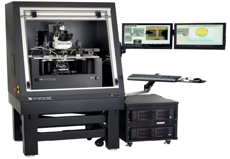 Complete MEMS Prober System - Showing Olympus Metallurgical / Biological Microscope Integrated with a 200 mm Semiautomatic Probe System
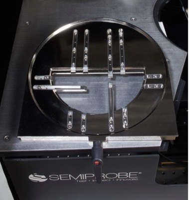
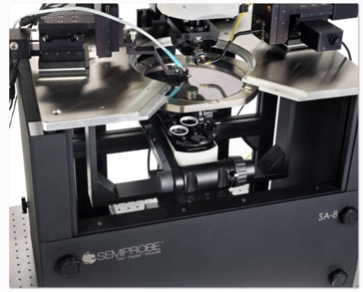 Programmable MEMS Manipulators with High-Frequency Probes
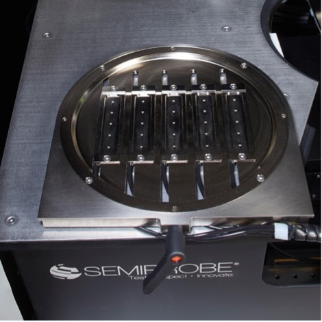
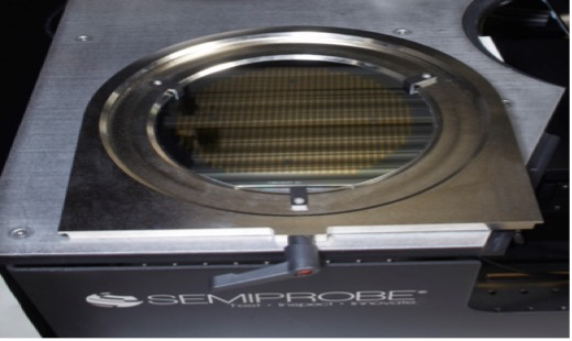 MEMS Wafer Carriers for Topside / Backside Testing
 Partial MEMS Wafer Carrier for Topside / Backside Testing
Individual Die Carrier for Topside / Backside Testing
Key MEMS Probe System Components:
- PS4L SA-8 semiautomatic probe system with programmable X,Y,Z, and theta stage
- Thermal Chuck System that operates from ambient to > 300 C
- Custom carriers for whole wafers, partial wafers, and individual die
- Customized Microfluidic Dispense System – input and output
- Four (4) programmable X,Y and Z manipulators with coaxial, triaxial and high frequency probe arms
- Probe Card Holder
- Test Instrumentation Rack and Cabling
- Customized Vibration Isolation Table, Dark Box and Dark Box Feedthrough Interconnect Panel
- Customized Graphical User Interface (GUI)