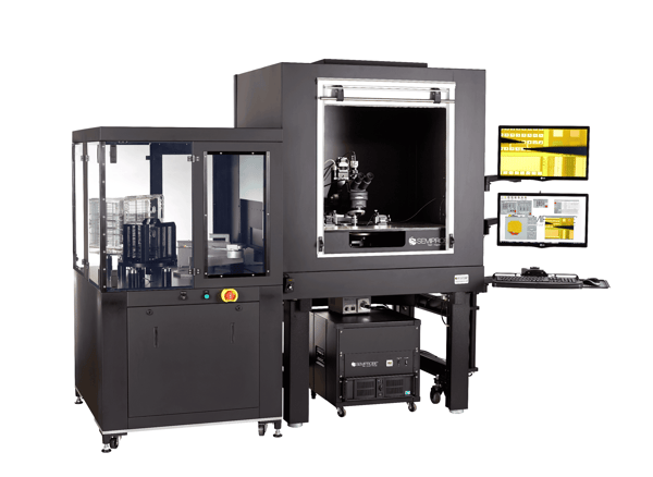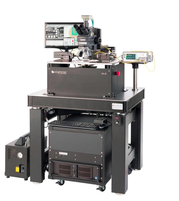
The semiconductor probe station is a well-established tool for testing circuits and devices on silicon wafers, dies, and open microchips. Two of the most commonly asked questions about probe stations are:
- What is a Probe Station used for?
Probe stations allow a user to position electrical, optical or RF probes on a silicon wafer so that the device can be tested. These tests can be simple, such as continuity or isolation check, or sophisticated, including full functional testing of microcircuits. Tests can be run either before or after the wafer has been sawn into individual dies.
Testing at the wafer level allows a manufacturer to test a device multiple times during the production process, which may provide insight as to which process steps are introducing defects into the finished product. It also enables manufacturers to test the dies prior to packaging, which is important in applications where the packaging costs are high relative to the device costs.
Finally, probe stations are often used in R&D, product development and failure analysis applications, where engineers need a flexible, precise tool to conduct tests on different areas on a device.
- How does a Probe Station work?
Probe stations provide a device to hold a wafer or die, and use a “Stage” to precisely position the device. Manipulators are placed on a planar surface, called the “Platen”. The user installs probe arms and tips into the manipulators and uses a microscope, mounted above the platen, to place the probe tips onto the correct locations on the device. Once all the probe tips have been set in their correct location, the device can be tested. For wafers with multiple dies, the user can then raise the platen, which will separate the probe tips from the die, then move the stage over to the next die, using the microscope to find the precise location. Since the dies are identical, once the stage is in position all of the probe tips will be properly located and the platen can be lowered, and the next die can be tested.
This is done by hand on manual systems. Semiautomatic and fully automatic systems use motorized stages and machine vision to automate this die to die movement process, increasing the productivity of the probe station and reducing the labor needed to run multiple tests.

For information on how to select a probe station, check out our "Tips and Tricks for Selecting an Analytical Probe System" blog.


