What is a Wafer Chuck?
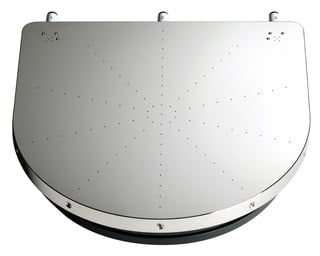
A wafer chuck is often used to hold wafers in place while they are being probed (tested). Most wafers are held in place by applying a small amount of vacuum to the backside of the wafer. The majority of analytical probing systems are provided with a a wafer chuck.
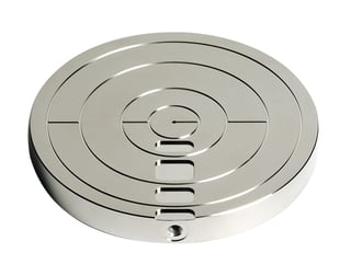
Wafer chucks are available in a variety of shapes, sizes and materials. They are typically round and are slightly larger then the wafer size. Common sizes range from 50 mm to over 300 mm in diameter. Most chucks have a circular (concentric) ring vacuum design and will often hold small die, partial wafers and whole wafers. For example, a 150 mm (6”) chuck will have vacuum ring patterns that will allow your to hold individual die, 50 mm, 75 mm, 100 mm and 150 mm wafers.
Most chucks are made of aluminum and have a nickel or gold plating. Sometimes chucks are made of steel, could be square and have a vacuum hole pattern instead of a vacuum ring pattern. Most chucks will have flatness specifications that range from +/- 4 um to +/- 8 um.
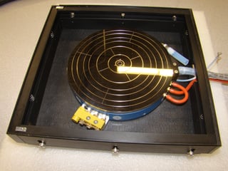
Chucks are often manufactured for specific applications. There are ambient chucks, high frequency/microwave chucks, high power (high voltage or high current) chucks, double-sided chucks and thermal chucks. It is not uncommon to make customized chucks.


