Quite often we get asked if we build test chambers.
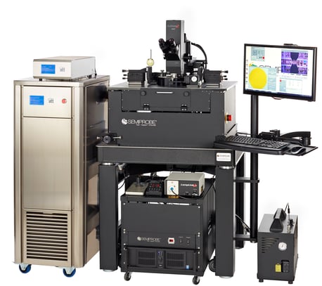 Example of a Semiconductor Wafer Probe System with a Localized Environmental Chamber
For some applications such as wafer probe and test the answer is yes but the chambers we manufacture are Localized Environmental Chambers (LEC) and Dark Boxes.
The LECS are integrated with our probe systems – manual, semiautomatic and fully automatic. They are primarily used to provide frost-free probing, light and EMI shielding. The device under test (DUT) is placed on a chuck that is enclosed by the LEC and LEC cover or top hat.
Dark Boxes are primarily used to provide a light-tight probing environment. The probe system is inserted inside the dark box. The dark box has a door that opens and closes and feedthrough panels that allow the cables to be connected or passed from outside to inside.
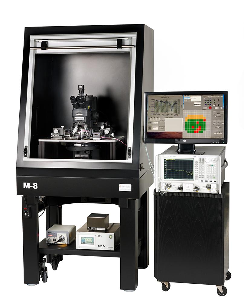
Semiconductor Wafer Probe Station Dark Box