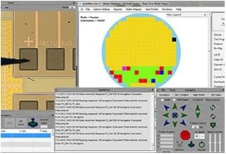
Wafer sort or sorting can be performed in a few different ways using analytical or production probing systems. Analytical probers are available in manual, semiautomatic and automatic configurations. Most production probers are automatic only. It all comes down to how many wafers need to be tested as well as how many samples (sample size) you want to test on each wafer.
Wafer sort can be performed in a few different areas of a semiconductor facility. In most cases it is performed soon after the wafers are moved out of the wafer fabrication area (Front-End). The wafers are usually fabricated in batches or lots that can range in size from a few wafers up to 48 or more. The batches are manufactured to a desired recipe or part number – diode, transistor, IC, etc. Wafer sort is an early determination of how well the wafer fabrication area did to meet the desired part number they were trying to make. The wafer sort test program often tests to multiple part numbers.
Example: For this article we will assume that a wafer fabrication site (company or foundry) received an order for 100,000 2N2222 transistors to be delivered in wafer form. To meet the requirements of the order a demand is placed on wafer fab to start a lot of twelve (12) 100 mm silicon wafers. A number of weeks later the wafers are finished in fab and are ready for test. The lot of twelve wafers are sent to wafer sort for multiple die testing. For this example we’ll assume that wafer sort has a manual prober connected to a tester – curve tracer, parametric analyzer, discrete or IC. The operator loads a wafer and then moves to a number of different locations on the wafer. The sample size and test locations can vary – 24 sites using the 4 corners and the diagonals as the test pattern. It is not uncommon to test for multiple part numbers at the same time. The test or binning results are printed on the wafer label and the label is affixed to the wafer cover. The process continues until all wafers have been sorted. The wafer sort results are reviewed and a decision is made on how many wafers are required for additional processing to fulfill the order (back grinding, backside metalization, 100% probe, visual inspection and Quality Control). Quality Control will randomly test a sample of the 2N2222 devices. If the outgoing QC testing passes the wafers get shipped to the customer and the order is fulfilled.
Wafer sort is a crucial process in semiconductor wafer processing facilities. It is the first testing stop for completed wafers. The test results provide valuable feedback to multiple departments – production control, wafer fabrication, product engineering and quality control. If yield results are low then changes have to be made. If yields are high or as expected the process is in control and no changes are required.
For more information on the Probe System for Life (PS4L,) please request a discovery call and someone from our team will be in touch.


