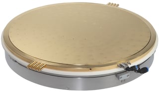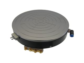
What are hot chucks?
Hot chucks, otherwise known as thermal chucks, are primarily used on probe systems (manual, semiautomatic or fully automatic) to heat or cool semiconductor wafers. They come in a variety of sizes ranging from 150 mm to 300 mm and are normally round with nickel or gold plating. Hot chucks are often provided with coaxial or triaxial connections to bias the wafer.
The most common temperature ranges are:
- Ambient (25 C) to 200C, 300 C or 400 C
- -40 C to 200 C or 300 C
- -60 C to 200 C or 300 C
Ambient to 200 C is the most highly requested temperature range, because elevated temperatures are easier to test and integrate with a probe system. Unlike ambient to 200 C, 300 C and 400 C often require special materials (thermal chuck adapters, cables, probe arms) and cooling (platens) to prevent the user from being exposed to hot surfaces.
Thermal chucks that provide cooling capabilities are often cooled using a chiller unit and a cooling fluid such as Galden, nitrogen, water or clean dry air (CDA). There are advantages and disadvantages to the various methods. Providing cooling capabilities on a probe station requires the thermal chuck to be shielded from ambient air and the most common method is a small chamber. The chamber prevents ambient air from entering the chamber and frosting up the chuck and device under test (DUT).
When integrated with a probe system, mounting the thermal chuck requires special attention. The extra cables and hoses used to heat and cool the thermal chuck create an additional drag on the wafer stage, which can impact movement and specifications (accuracy, repeatability and resolution). A complete thermal chuck system requires a chuck, a control unit and a cooling unit.
There are a few worldwide suppliers of thermal chucks. For more information, fill out the form or request a discovery call


