Turnkey and Integrated 200 mm Semiautomatic Probe System with an Olympus Metallurgical Microscope for a large Wafer Foundry
Customer Requirements:
- Complete turnkey and integrated wafer probing system to test a variety of MEMS technologies in whole wafer, partial wafer and die form over temperature.
- Integrated solution had to provide a fully functional topside and bottom side wafer probing and high magnification inspection capabilities using one platform and in a dark box
- Programmable Manipulators with HF and DC probe arms for electrical testing and fluidic dispense
- The devices needed to be heated and monitored from ambient to > 300 degrees.
- All test instrumentation, cables, connectors and a Graphical User Interface (GUI) had to be provided
SemiProbe Solution:
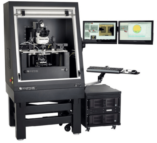
Semiautomatic multi-application MEMS Prober with programmable manipulators, thermal chuck, Olympus metallurgical microscope, dark box, and vibration isolation table
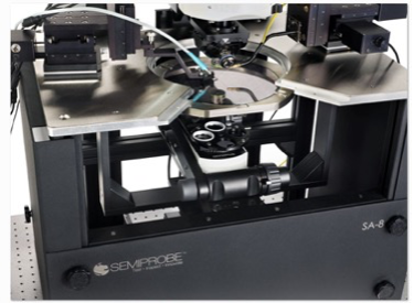
Programmable Manipulators with High Frequency and Triaxial Probe Arms with DSP wafer chuck
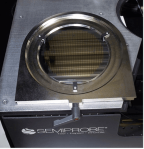
DSP Wafer Carrier
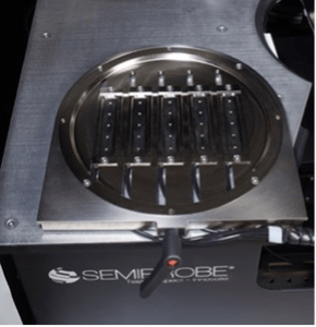
DSP Chip Carrier for individual die
Whole wafers, partial wafers, and individual die can be probed on the system using manipulators or a probe card. The devices are inserted in customized carriers and are held in place via mechanical clamping. The devices can be loaded on an adjacent bench or table and are easily inserted into and removed from the chuck assembly.
Key System Components:
- PS4L SA-8 semiautomatic probe system with programmable X,Y,Z, and theta stage
- 200 mm thermal chuck system that operates from ambient to > 300 C
- Custom carriers for whole wafers, partial wafers, and individual die
- Customized Microfluidic Dispense System – input and output
- Four (4) programmable manipulators with coaxial, triaxial and high-frequency probe arms
- Probe Card Holder
- Test Instrumentation Rack and Cabling
- Customized Vibration Isolation Table, Dark Box, and Dark Box Feedthrough Interconnect Panel
- Customized Graphical User Interface (GUI)