

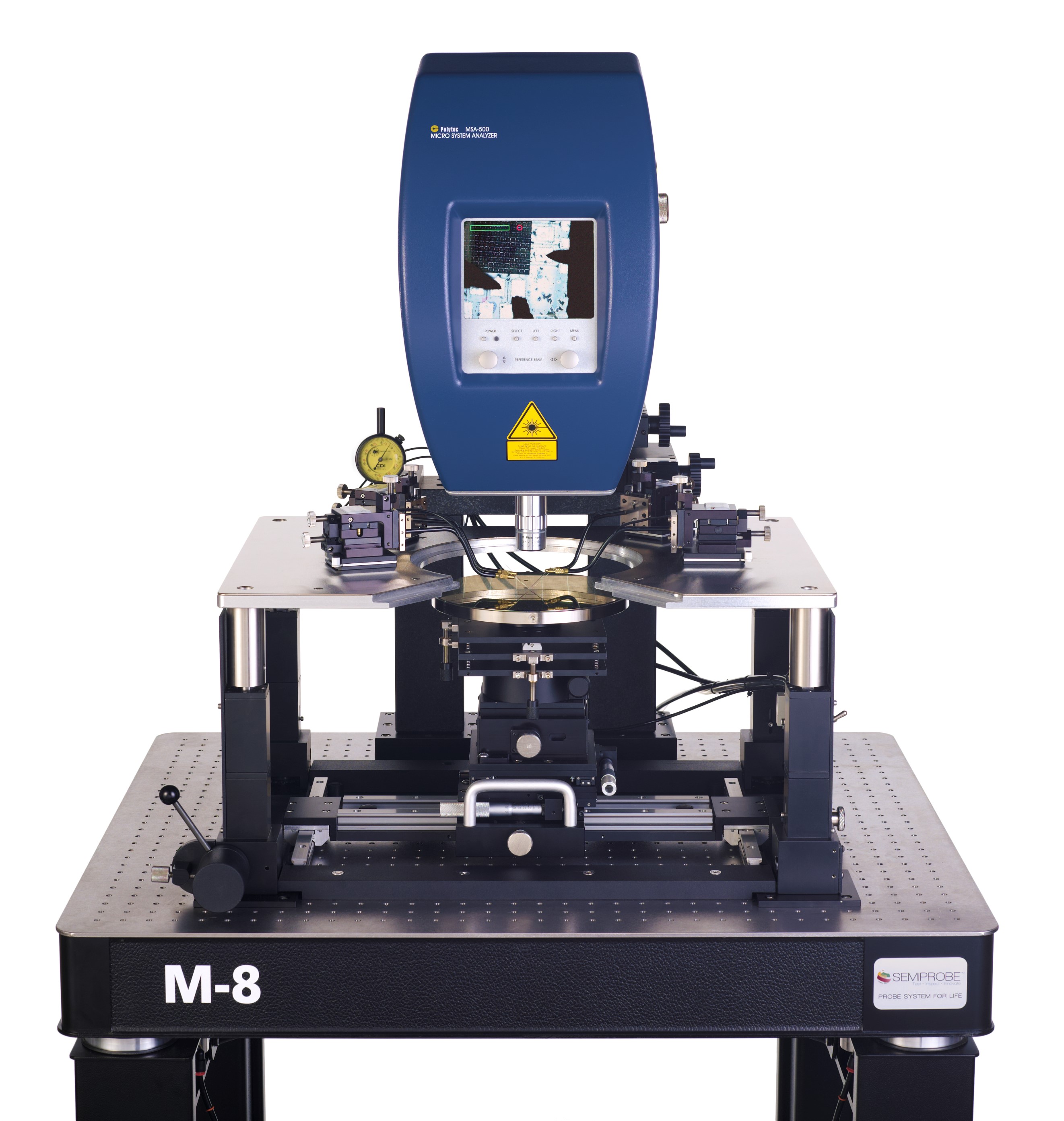
The customer wanted to test 200 mm silicon MEMS wafers using a manual probe system integrated with a Polytec MSA-500 MEMS Motion Analyzer. The motion analyzer would measure a variety of MEMS devices while in-plane and out-of-plane. The wafer chuck would need to be tilted in a variety of directions. The devices would be contacted with a probe card as well as individual manipulators with coaxial probe arms and DC probe needles.
To learn more about this wafer probe Click Here
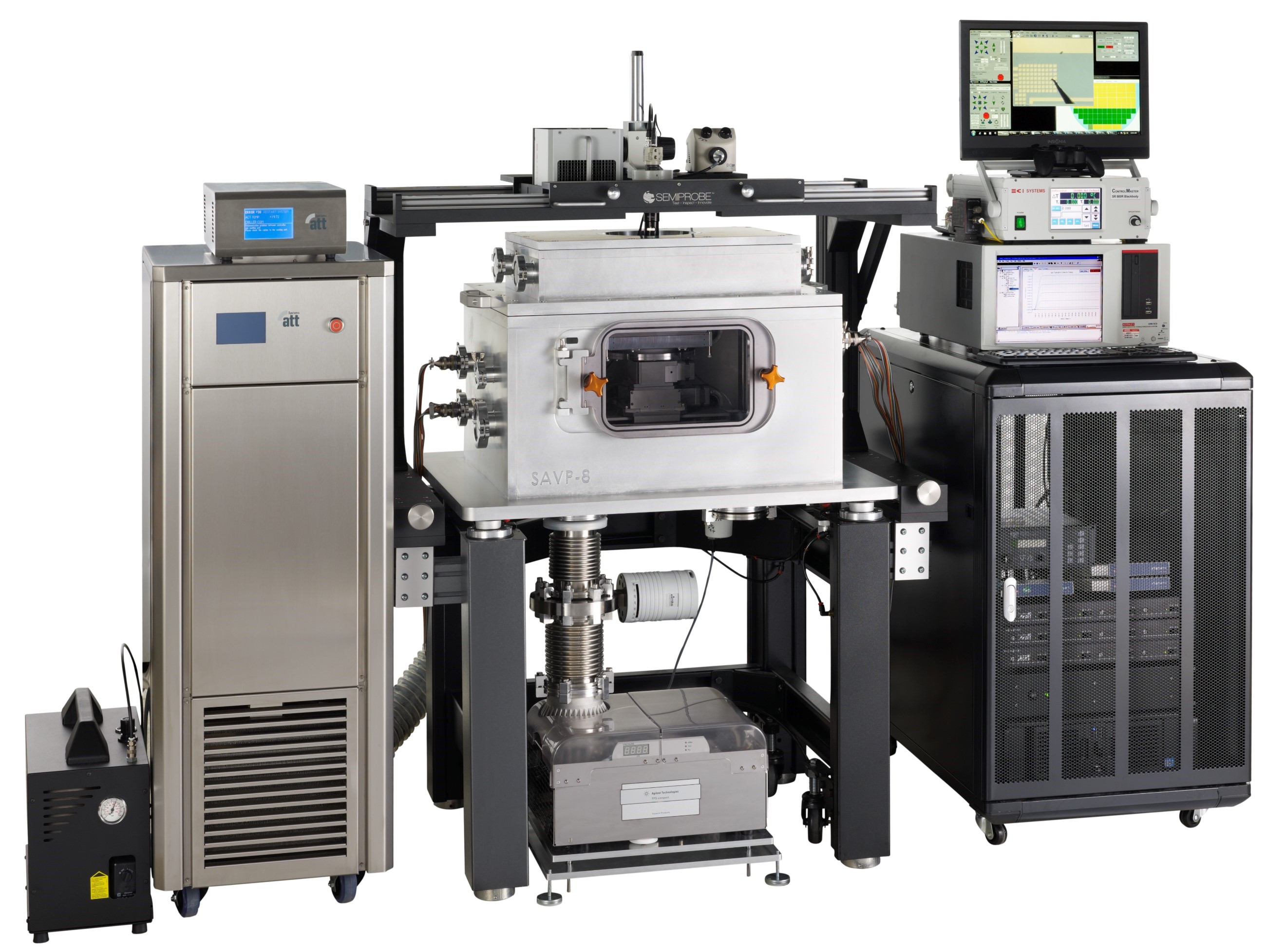
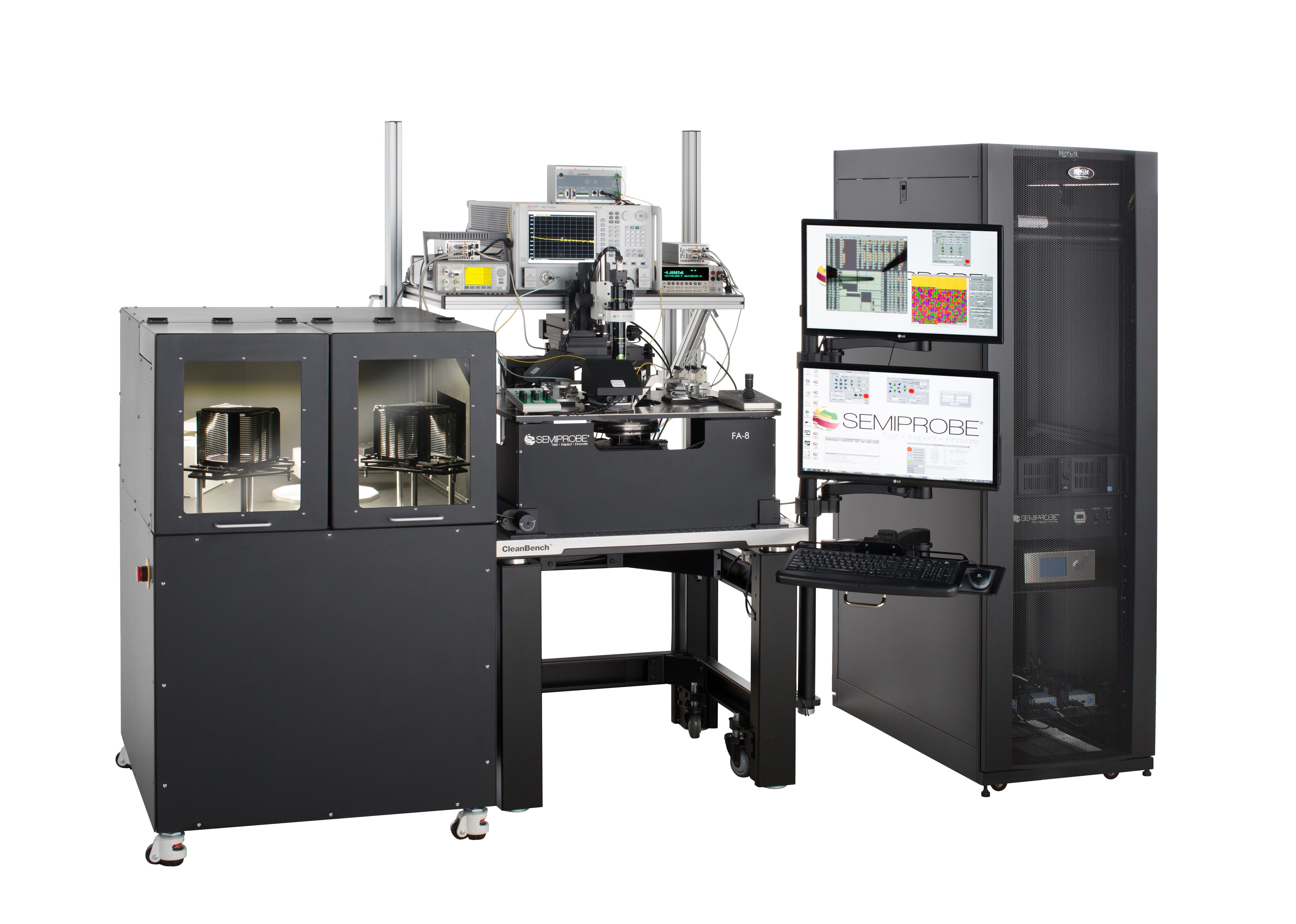
The customer wanted to test 200 mm silicon MEMS wafers under vacuum. They wanted the ability to test at low and high temperatures (-60 C to 200 C). They wanted the ability to use probe cards as well as programmable manipulators with DC and High Frequency (HF) probe arms. The probe system would need the ability to interface to a variety of Keithley and Keysight test instrumentation. The microscope bridge needed the ability to support optics, black bodies and a Polytec MEMS motion analyzer.
To learn more about this Wafer Prober Click Here
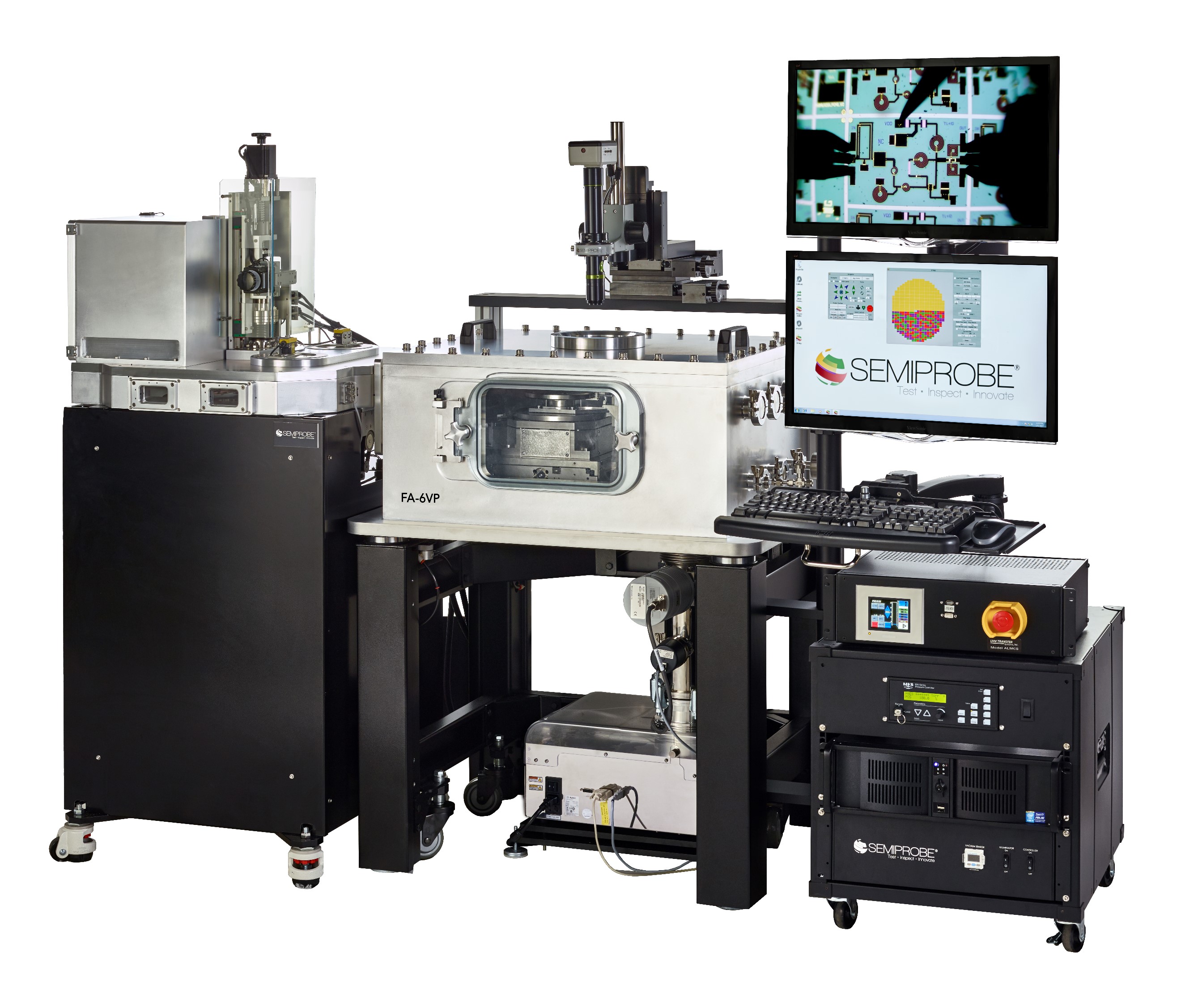
The customer wanted to test 150 mm silicon MEMS wafers in a fully automatic mode under vacuum. The wafers would be mounted in a single cassette into a material handling chamber with a load lock. The material handling unit (MHU) would remove a wafer from the cassette and place it on a mechanically clamping chuck mounted on the probe system vacuum stage in the After alignment the device testing would be performed using a probe card or individual programmable manipulators with DC and High Frequency (HF) probe arms and probes. Everything within the chamber would need to be vacuum compatible.
To learn more about this Wafer Prober Click Here
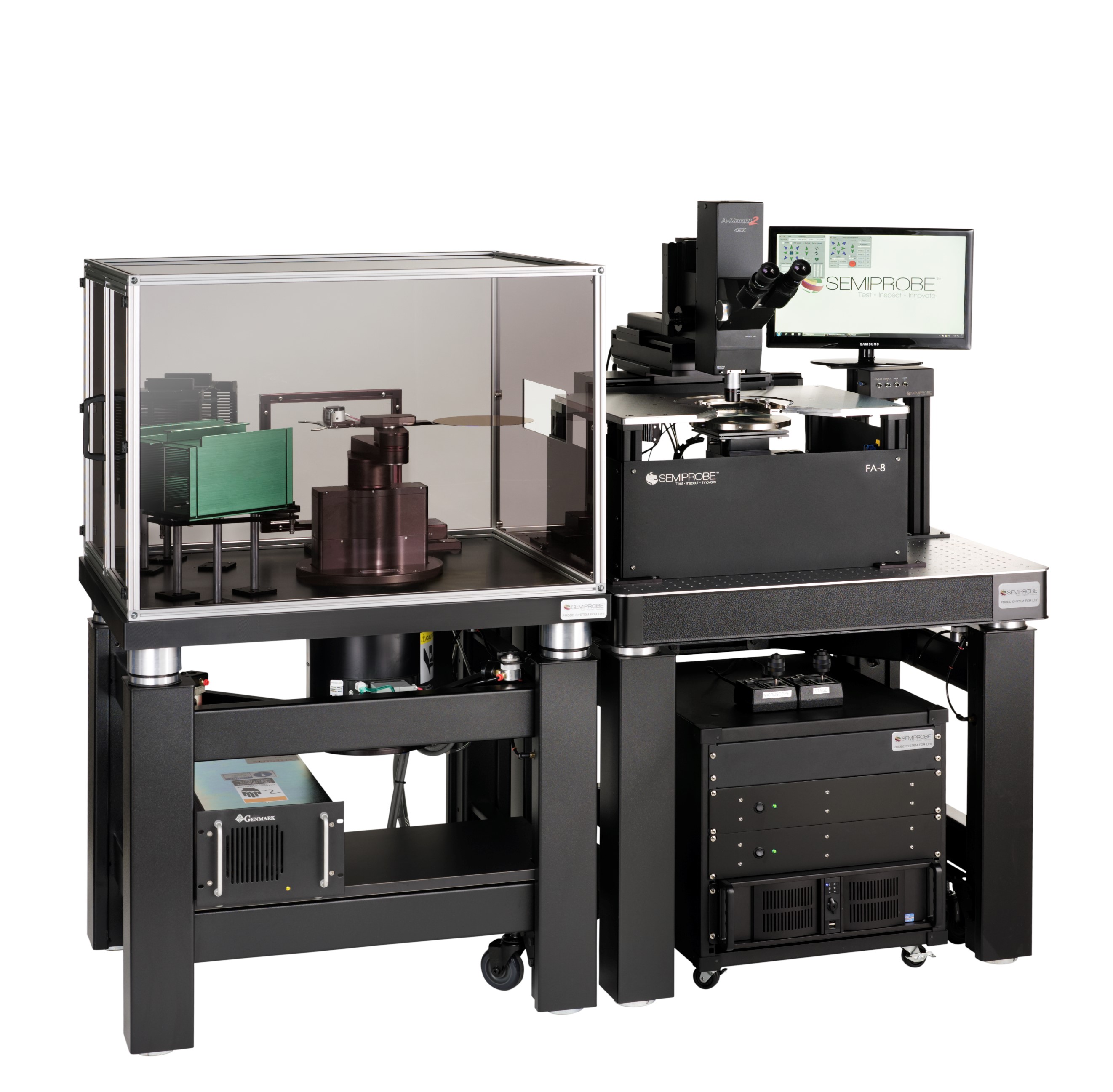
The customer wanted a highly flexible fully automatic 200 mm probe system for MEMS production. The system had to have the ability to handle wafers (100 mm, 150 mm and 200 mm), wafers mounted on frames and trays of die. The system had to provide the ability to be operated in manual, semiautomatic and fully automatic modes. The system had to operate with probe cards and manipulators.
To learn more about this wafer prober Click Here
Customer Requirements:
The customer wanted a fully automatic probe system to test silicon photonic devices in wafer form that were manufactured using MEMS technology. Due to small pitches and tight tolerances the customer needed four (4) programmable manipulators. Two (2) manipulators were multi-axis hexapods and two (2) were three-axis manipulators. The two hexapod manipulators had probe arms that could handle single and multi-mode fibers. The fiber needed to be placed within 10 um of the device surface so non-contact height measurement sensors were required and mounted to the fiber arms. The two (2) three-axis manipulators used single DC or High Frequency (HF) probe arms with the appropriate probe tips.
To learn more about this Wafer Prober Click Here