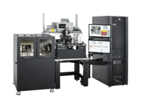
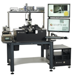
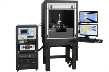
The never ending quest for more capable optoelectronic devices are challenging the prober companies to develop new methods of holding, integrating products and testing a variety of devices ranging from individual chips, modules, partial wafers and whole wafers up to 300 mm in size.
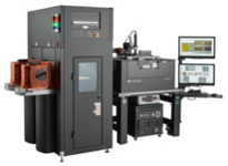
Optoelectronic Probing solutions range from R&D to Production. Some recent trends:
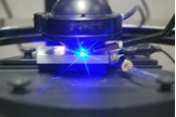
- Topside and Bottomside Bias or light detection
- Stimulate/Bias from the topside of the device, detect light output from the backside
- Stimulate/Bias from the backside and detect light from the topside
- Simultaneously probe from the topside and backside
- Stimulate from the topside and detect light output from the side(s)
- Cold and Hot temperature testing in a double-sided probing application
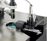
- Non-Contact Height Measurement Sensors to precisely control the fiber location in regards to the device under test (DUT)
- Integration of multi-axis Hexapods with fibers (single or multiple) with light optimization
- Moving from a single-purpose probing solution to a multi-purpose probing solution
- Providing turn-key probing and testing solutions
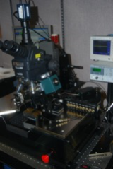
A large family of optoelectronic devices need to be tested on the probe systems – LEDS, VCSELS, EELDS, Silicon Photonics and more. Optoelectronics testing often requires a combination of stimulus using manipulators (manual or programmable) with DC probes, High Freqency probes, Optical Fibers and multi-contact wedges. Sometimes probe cards are used to stimulate from the top, bottom or both sides at a time. It is not uncommon to test a Silicon Photonics MEMS device that requires DC, High Frequency and Optical stimulus at the same time.
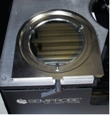
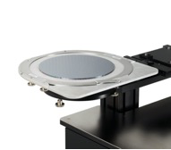
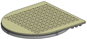
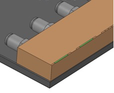
The devices are not always in wafer form and it is not uncommon for customers to want to test individual die, trays of die, modules, partial/broken wafers and wafers sawn and stretched on frames (metal or plastic) using the same probe system. To do this requires a large selection of fixtures and carriers to be developed. Some of the fixtures use vaccum to hold the devices and others require mechanical clamping. Fixtures are often designed to be universal to hold a variety of die sizes as well as simultaneously hold both VCSELS and EELDS. Some fixtures need to be isolated from the chuck (standard or thermal) or conductive with a gold or nickle plating.
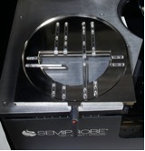
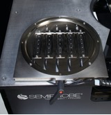
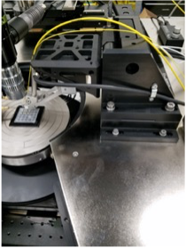
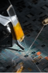
Output light collection is often with a fiber or an integrating sphere. The fibers are usually mounted to a manipulator (manual or programmable) or a programmable stage (X,Y and Z) used in double sided probing applications. Flexible mounting of the fibers is required to accommodate a large selection of fiber sizes, arrays and angles. It is not uncommon to have a universal fiber holder that allows the fiber to be changed for VCSEL and EELD testing.
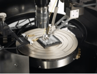
Integrating spheres are made by a few different manufacturers and come in a variety of sizes. Most used in probing solutions range in size from 2” (individual devices) to 6” (arrays) diameters. They are integrated with the probe system and can be mounted in a few different areas – rear, side and front. Moving the integrating sphere in and out of position can be done in a few modes - manual, pneumatic or programmable. For some applications they can be fixtured to allow VCSELS as well as EELDS to be tested using the same integrating sphere.