What are probe cards and when are they used with a probe system?
Probe cards are primarily used to probe semiconductor devices, and there are many different types, sizes and worldwide manufacturers.
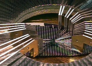
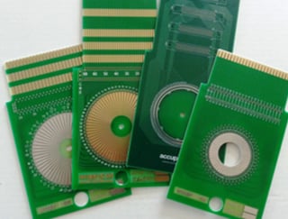
This article specifically talks about probe cards with cantilevered probe tips that vary in width from 4.5” to 6” and have probes that protrude below the top surface of the card. The probes are usually mounted and soldered to a trace onto a printed circuit board, and they can be used with manual, semiautomatic or fully automatic probe systems.
Probe cards can be simple with just one probe (diode) or can be complex with hundreds or even thousands of probes for integrated circuit or simultaneous multi-site testing requirements. The cable connections to the probe card are usually edge finger (up to 48 pins) or ribbon cable (up to 160 pins).
A few of the most common reasons for using a probe card are:
- Manipulator Limits – Without a probe card, a typical prober can only place a limited number of manual manipulators around the platen opening - 8 to 12. Additionally, the operator has to make manual adjustments for each individual probe tip, which can be a tedious process that requires quite a bit of experience and time.
- Device layout – Probe cards are useful when the user wants to probe devices with high pin counts (>12).
- Production – Probe cards are primarily used for production probing applications. Production applications can range from a simple diode of one probe to integrated circuits that use several hundred probes.
How to get a probe card built?
Probe cards are built to match the number of probes with the number of pads on the device under test (DUT). To get a probe card built, the user supplies the probe card manufacturer with the mechanical drawings of the device layout or a sample of the device.
To stay up to date with the latest semiconductor and probing solutions news, subscribe to the SemiProbe blog.

Probe card photographs courtesy of Accuprobe – www.accuprobe.com


