Customer Requirements:
- The customer had 150 mm and 200 mm wafers with RF components that needed to be tested over a temperature range of -60 C to 300 C. They needed the ability to perform 2-port, 3-port and 4-port measurements using a Keysight Vector Network Analyzer.
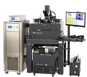
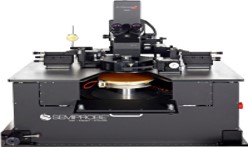
RF Probe Station Solution
Key System Components:
- 200 mm semiautomatic RF Probe Station with a programmable X,Y, Z and theta wafer stage
- 200 mm thermal chuck system that operates from – 60 C to 300 C with gold plated RF add-on surface
- A localized environmental chamber (LEC) with a top hat to provide light tight, EMI shielded and frost-free probing
- Compound Optics Bridge with 50 mm x 50 mm x 80 mm of Compound Optics Movement and Compound Optics with motorized zoom
- Four (4) manual MA-8500 manipulators with West/East and North/South RF probe arms with 40 GHz and 65 GHz RF probes, calibration substrate and cables.
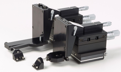
- Two (2) MA-8100 manipulators with coaxial probe arms for DC bias
- PILOT Software Suite (Navigator, Wafer Map and Autoalign)
- Vibration Isolation Table (VIT) with adjustable Monitor/Keyboard/Mouse Rack
- Small footprint and quiet air compressor for the VIT and pneumatic microscope lift