Customer Device Characterization Requirements:
A highly configurable 200 mm semiautomatic device characterization probe system that would interface to a Keysight B1500 and controlled via their EasyExpert software. The probe system had to operate from -60 to 200 C, providing the ability to make multiple types of measurements – low leakage, low capacitance, low voltage, and low resistance as well as high frequency.
High magnification optics to see features in the micron range were required as well as a family of manual and programmable manipulators manufactured by SemiProbe and Imina Technologies to contact pads and sub-micron features.
SemiProbe Device Characterization Solution:
Key Device Characterization System Components:
Built using SemiProbe’ s patented Probe System for Life (PS4L) Adaptive Architecture consisting of:
- A TMC vibration isolation table (VIT) with casters, leveling feet and adjustable keyboard/monitor rack
- A 200 mm programmable X, Y,Z, and Theta stage with control electronics
- A 200 mm, gold plated triaxial thermal chuck with vacuum holes that operates from -60 C to 200 C that is mounted to a large travel load-stroke for easy device loading and unloading
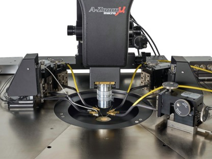
- A localized environmental chamber (LEC) with top hat to provide frost-free, dark and EMI shielding
- A linear platen lift that provides course and fine platen movement in Z
- A large aluminum platen with stainless steel skin that has a removable front wedge. Platen allows manipulators to be placed anywhere around the platen opening.
- A second and recessed platen for the addition of multiple Imina Technologies miBot nanopositioners
- A compound microscope bridge with a 50 mm x 50 mm x 80 mm X, Y and Z travel
- Compound Microscope with 2x, 10x, 20x, 50x and 100x objectives
- A CCTV System consisting of a color camera, color monitor, c-mount camera adapter, and cables
- PC/Monitor, GPIB, and PILOT Software Suite (Navigator, Wafer Map, Autoalign)
- Four (4) programmable three-axis (X,Y, Z) manipulators with coaxial and triaxial probe arms
- Four (4) manual manipulators with coaxial, triaxial, and Kelvin probe arms
- One (1) manual manipulator with contact sense probe
- Assorted boxes of tungsten probe tips (12.5 um, 7 um, 1 um, and 0.1 um radius)
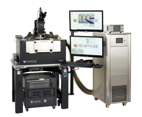 Semiautomatic 200 mm Device Characterization Prober System configured with manual and programmable manipulators, a localized environmental chamber, and a thermal chuck system that operates from -60 C to 200 C
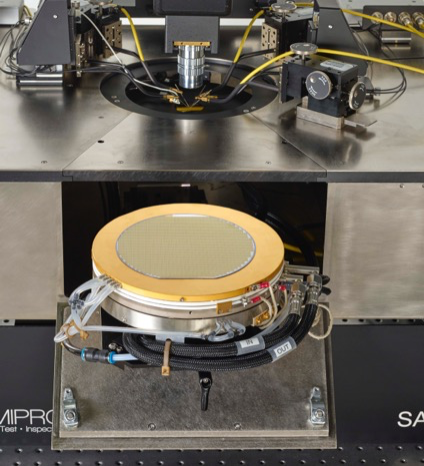
Localized Environmental Chamber (LEC) with triaxial thermal chuck in the load position
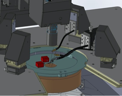
Manual, Programmable, and Imina miBot nanopositioners integrated into a single probing platform