Customer Requirements:
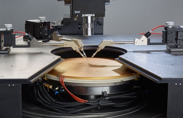
- The customer is involved with the CERN Program and required a flexible 300 mm semiautomatic system to test high voltage sensor arrays and a variety of other devices. The system would need high and low temperature capabilities. Manual manipulators with a few different standard as well as high voltage (HV) probe arms were required. The system needed the ability to test devices that ranged from 1 kV to 10 kV. The system would get interfaced to Keysight B1505 test instrumentation.
SemiProbe Solution:
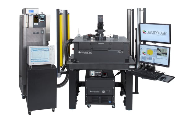
- A PS4L SA-12 (300 mm) semiautomatic probe system
- A 305 mm x 305 mm programmable X,Y and Z wafer stage
- A 300 mm thermal chuck with a triaxial HV addon surface that operated from -60 C to 200 C.
- A localized environmental chamber (LEC) with a top hat
- Compound Microscope Bridge with a 50 mm x 50 mm X and Y microscope movement and an 80 mm pneumatic Z lift
- Compound Optics and CCTV System
- PC/Monitors/Keyboard/with adjustable rack
- PILOT Software Suite – Navigator, Wafer Map and Autoalign
- Six (6) manual manipulators with a variety of probe arms – coax, triax and high voltage (3 kV and 10 kV)
- Vibration Isolation Table (VIT) with a Laser Light Safety Curtain
- Interlock Panel – mounted to the plexiglass cover and contains a variety of feedthroughs and safety interlock