Success Story – Optoelectronics - Europe
Custom Optoelectronic Test System - Vtt (Finland) Customer Requirements:
- Fully Automatic Electro-Optical probing system for high volume production to measure waveguide structures on silicon wafers plus other data launching/light collection through integrated coupling mirrors.
- The system handles 100 mm and 150 mm wafers automatically and be able to operate in manual, semiautomatic and automatic modes.
- The system automatically reads the device height and accurately maintain a fiber within 10 um of the device under test.
- The system is integrated with four (4) programmable manipulators. Two (2) six (6) axis SmartActs with fiber holders and two (2) are three (3) axis Physik Instrumente (PI) manipulators with High Frequency 40 GHz Ground-Signal-Ground (GSG) probes.
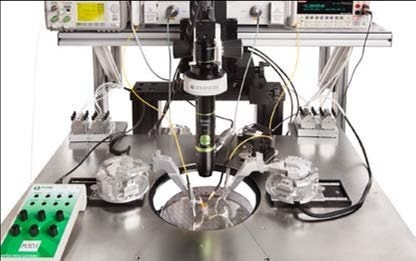
Multi-Axis programmable manipulators with integrated height measurement sensors and fiber optics
Fully Automated Electro-Optical Probing System with Test Instrumentation
Multi-Purpose Probing Application Involving Fiber Optics, High Frequency, and DC Probe Tips
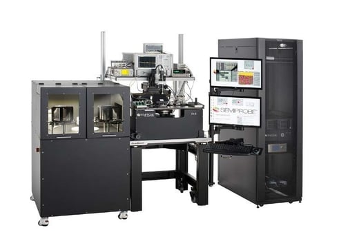
SemiProbe Solution:
Key System Components:
- Probe System for Life (PS4L) SA-6 semiautomatic probe system with programmable X, Y, Z and theta stage
- Ambient chuck with lift pins for material handling unit (MHU)
- Zoom Tube optics with CCTV System
- Two (2) programmable six axis SmartAct manipulators with customized probe arms for optical fiber and height measurement sensor
- Two (2) programmable three axis (X, Y and Z) PI manipulators with HF probe arms
- Height Measurement Sensors – two (2) with feedback system
- Material Handling Unit – robotic arm with end-effector, pre-aligner, two (2) cassettes each for 100 mm and 150 mm wafers, enclosure with interlocks
- PILOT Software Suite - Navigator, Wafer Map, Auto-Align, Programmable Manipulators, MHU
- Test Instrumentation Racks – two (2) - adjustable located at rear of prober to minimize test instrumentation cable lengths and adjacent to prober (manipulator and prober control electronics, PC)
Customer Testimonial:
VTT has developed Silicon Photonics since 1997 and is therefore one of the pioneers in this field. The capability to perform simultaneous E/O tests at wafer level while providing fast data collection for analytics, is instrumental for VTT to offer improved manufacturing and testing services to its customers.
"We are excited to use the cassette-to-cassette automatic PS4L probing station where we contribute applying our unique fiber probing and alignment know-how “ says Giovanni Delrosso, Sr. Scientist and Project Manager at VTT's Photonics Integration team in Espoo.
To learn about more advanced Optoelectronic Wafer Probers Click Here