Customer Requirements:
A USA automotive manufacturer required a small footprint and flexible high current probing solution that would allow them to test 100 mm wafers, chips and packaged parts up to 200 amps. Volume was low so a manual high current probe system with manual manipulators and a variety of high current (HC) and low voltage DC probe arms were desired. The high current probe system would get interfaced to a Keysight B1506. Due to the lethal voltage levels required to test the devices, a safety enclosure would be required.
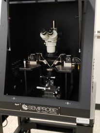
High Current Manual Prober with Dark Box Safety Enclosure
SemiProbe Solution:
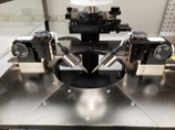
- LA-100 (100 mm) Lab Assistant manual high current probe system
- 100 mm wafer chuck with High Voltage (HC) and 3 KV triaxial force and sense connections
- Microscope Post with Coaxial X and Y Microscope Movement of 100 mm x 100 mm with locking knobs
- Compound Optics with CCTV System
- Two (2) MA-9100 manual manipulators with high current probe arms and one (1) MA-8005 with a coaxial DC probe arm
- Dark Box with door safety interlocks
- Interconnect Panel – contains standard coaxial, triaxial, and 3 KV HV (force and sense) triaxial connectors and adjustable rubberized boot for direct pass through of cables and Keysight boxes and safety interlock
Manual Manipulators with High Current Probe Arms
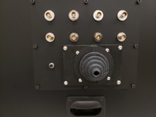
High Current and High Voltage Prober Interface Panel
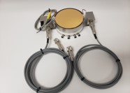
High Current Probe System Ambient Chuck with High Current and Triaxial Kelvin Connections

