Customer Requirements:
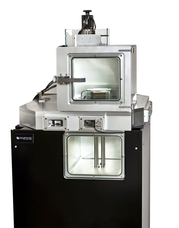
The customer wanted to test 150 mm silicon MEMS wafers in a fully automatic mode under vacuum. The wafers would be mounted in a single cassette into a material handling chamber with a load lock. The material handling unit (MHU) would remove a wafer from the cassette and place it on a mechanically clamping chuck mounted on the probe system vacuum stage in the After alignment the device testing would be performed using a probe card or individual programmable manipulators with DC and High Frequency (HF) probe arms and probes. Everything within the chamber would need to be vacuum compatible.
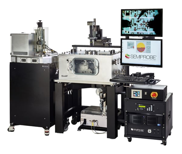
Fully Automatic Vacuum Probing System
- FA-6 – 150 mm fully automatic probe system
- 150 mm programmable X,Y,Z and theta stage
- PILOT Software Suite – Navigator, Wafer Map, Autoalign and MHU Modules
- Vibration Isolation Table
- All Components in the vacuum chamber rated to 10-6 torr
- Agilent turbo-molecular vacuum pump
- Probe Card Holder (PCH) and Probe Card
- Four (4) Programmable three axis manipulators with DC and HF probe arms, cables and probes
- Material Handling Unit (MHU) – one (1) 150 mm cassette, pre-aligner and end-effector
- Compound Optics with CCTV System
To learn more about advanced MEMS Wafer Probers Click Here.