Customer Requirements:
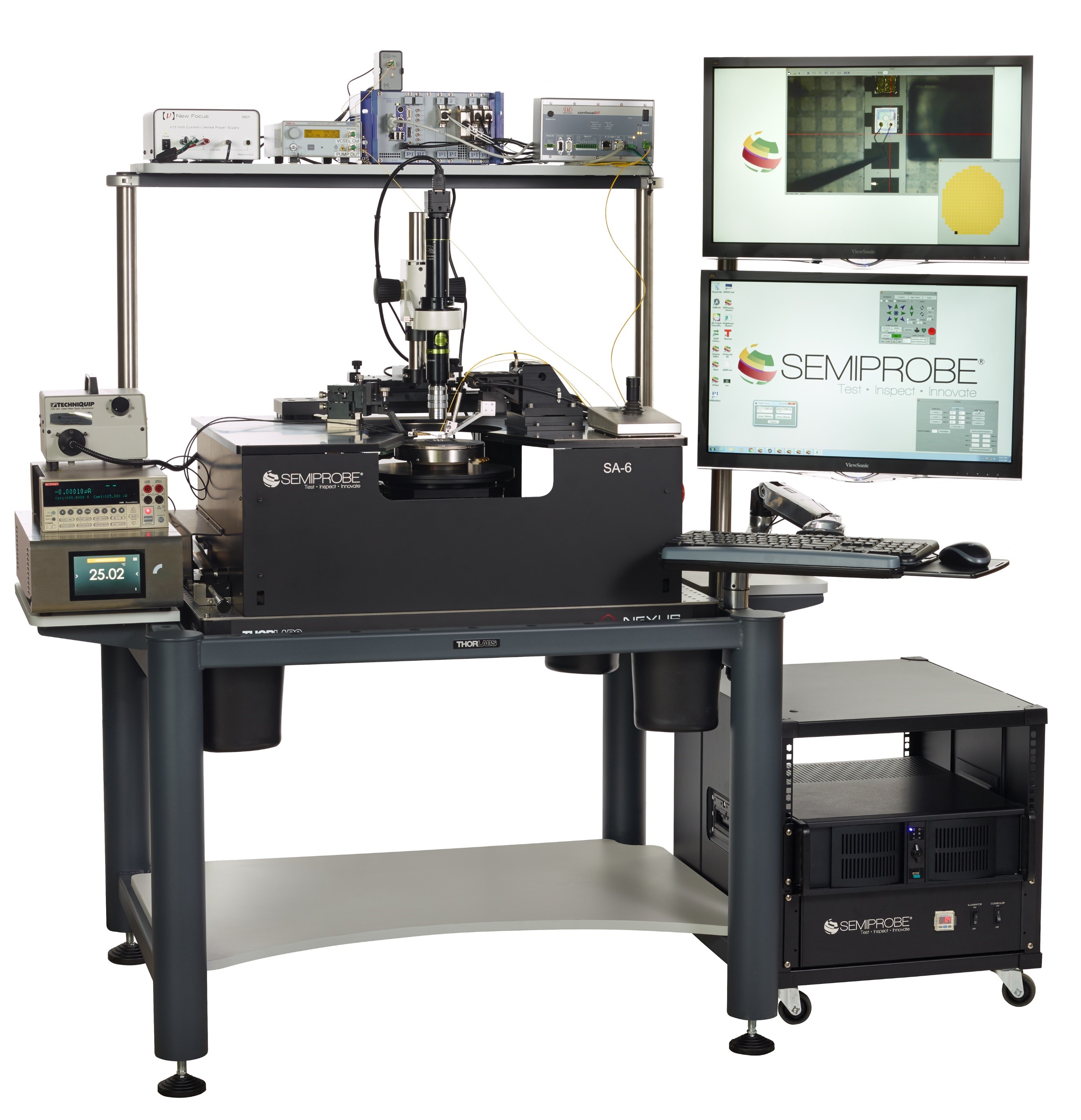
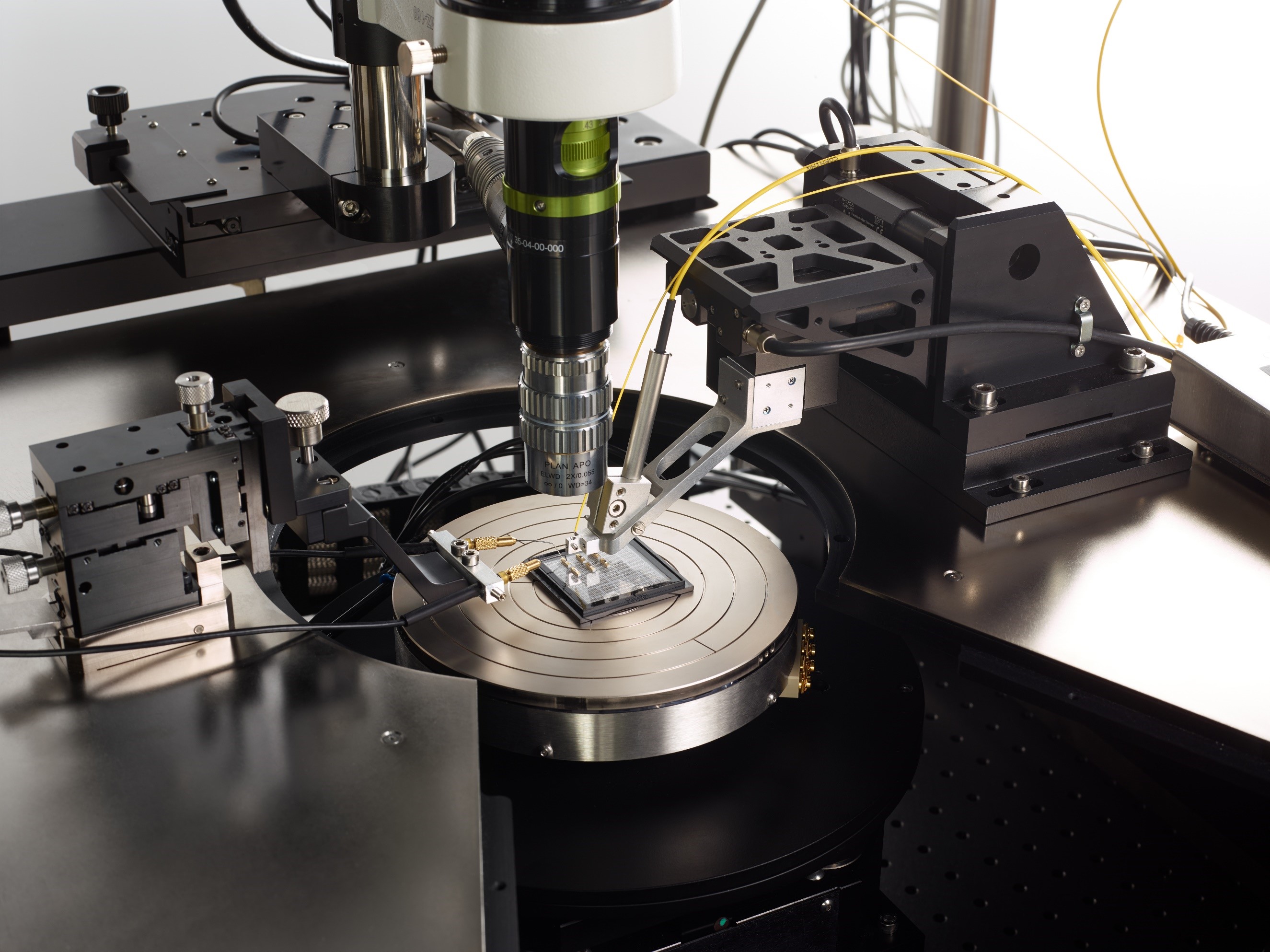
The customer wanted a 150 mm semiautomatic probe system to test vertical cavity surface-emitting laser diodes (VCSELS). The VCSELS were in wafer and individual die form and tested at temperatures ranging from 25 C to 200 C. The customer required the device to be biased from the top and bottom. A manual manipulator with a multi-contact DC wedge was used for biasing. A second manual manipulator was used for a non-contact height measurement sensor. An optical fiber was required to collect the light and it needed to be mounted to a three-axis programmable manipulator with a goniometer.
SemiProbe Solution:
Vertical Cavity Surface Emitting Laser Diodes (VCSELS)
- SA-6 Semiautomatic Probe System
- 150 mm programmable X,Y,Z and Theta stage
- PILOT Software Suite – Navigator, Wafer Map and Autoalign
- Vibration Isolation Table with Test Instrumentation Rack
- 150 mm thermal chuck – ambient to 200 C
- PI three (3) axis programmable manipulator with goniometer used for fiber
- DC manipulator with multi-contact DC wedge
- Optical fiber arm with Non-Contact Height Measurement Sensor
- Zoom Tube optics with CCTV System
To learn more about Advanced Optoelectronic Wafer Probers Click Here.