Customer Requirements:
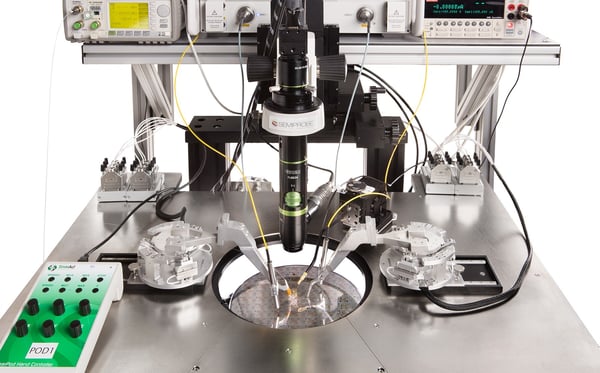
The customer wanted a fully automatic probe system to test silicon photonic devices in wafer form that were manufactured using MEMS technology. Due to small pitches and tight tolerances the customer needed four (4) programmable manipulators. Two (2) manipulators were multi-axis hexapods and two (2) were three-axis manipulators. The two hexapod manipulators had probe arms that could handle single and multi-mode fibers. The fiber needed to be placed within 10 um of the device surface so non-contact height measurement sensors were required and mounted to the fiber arms. The two (2) three-axis manipulators used single DC or High Frequency (HF) probe arms with the appropriate probe tips.
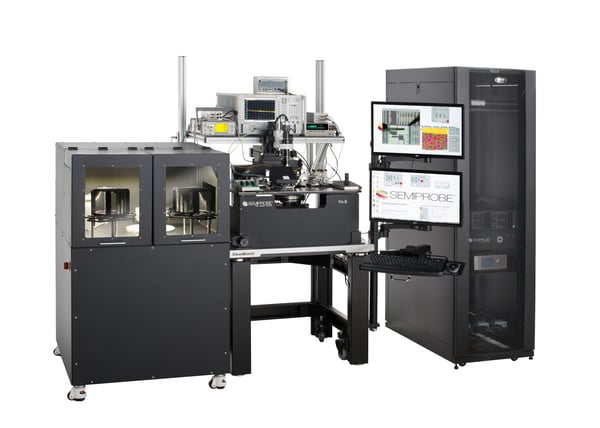
SemiProbe Solution:
- FA-6 - Fully Automatic 150 mm probe system
- 150 mm programmable X,Y,Z and theta stage
- PILOT Software Suite – Navigator, Wafer Map and Autoalign
- Four (4) Programmable Manipulators
- Two (2) multi-axis Smartacts for light input and output optimization
- Two (2) three axis manipulators with DC & HF probes
- HF, DC and Opto probe arms and probes
- Non-Contact Height Measurement Sensor
- Material Handling Unit
- Two (2) Cassettes, pre-aligner, scanner, bar code reader
- Test Instrumentation Racks
To learn more about Advanced Optoelectronic Wafer Probers Click Here.