Customer Requirements:
Using a semiautomatic 150 mm probe system the customer wanted to test light emitting diodes (LEDS) in wafer form, on 150 mm and 200 mm metal frames and plastic rings. The wafers needed to be tested from ambient to 200 C using a thermal chuck. The LED device would be tested using probe cards and stimulated from the top and bottom. The light output would be captured by an integrating sphere (cube) mounted on multi-axis pneumatically controlled stages that allowed the integrating sphere to moved in and out of position and up and out of the way for changeovers. Customized fixturing to address all of the requirements were required.
 SemiProbe Solution:
Light Emitting Diodes (LEDS)
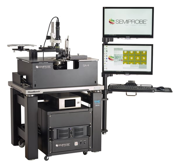
- SA-6 Semiautomatic Probe System
- 150 mm programmable X,Y,Z and theta stage
- PILOT Software Suite – Navigator, Wafer Map and Autoalign
- Vibration Isolation Table
- 150 mm thermal chuck operating from ambient to 200 C
- Customized metal and plastic ring frame holders with quick disconnect hardware for easy changeovers
- Ability to test whole wafers, partial wafers, individual die and wafers sawn & stretched on rings or frames
- Integrating Sphere mounted on a multi-axis stage to provide pneumatically controlled sphere movement
- Probe Card Holder
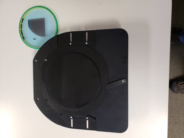
Universal Frame Mount
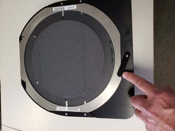
Frame Carrier
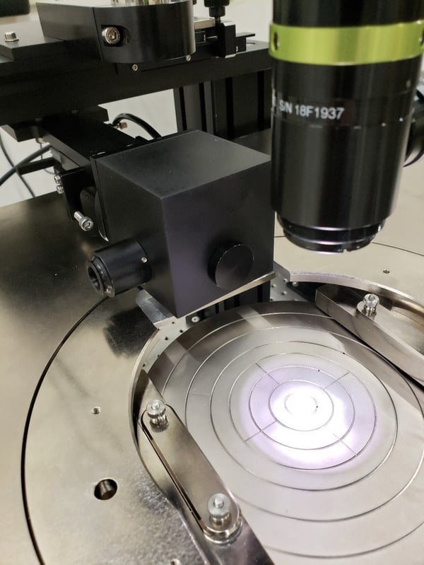
Integrating Sphere
To learn more about other Advanced Optoelectronic Wafer Probers Click Here