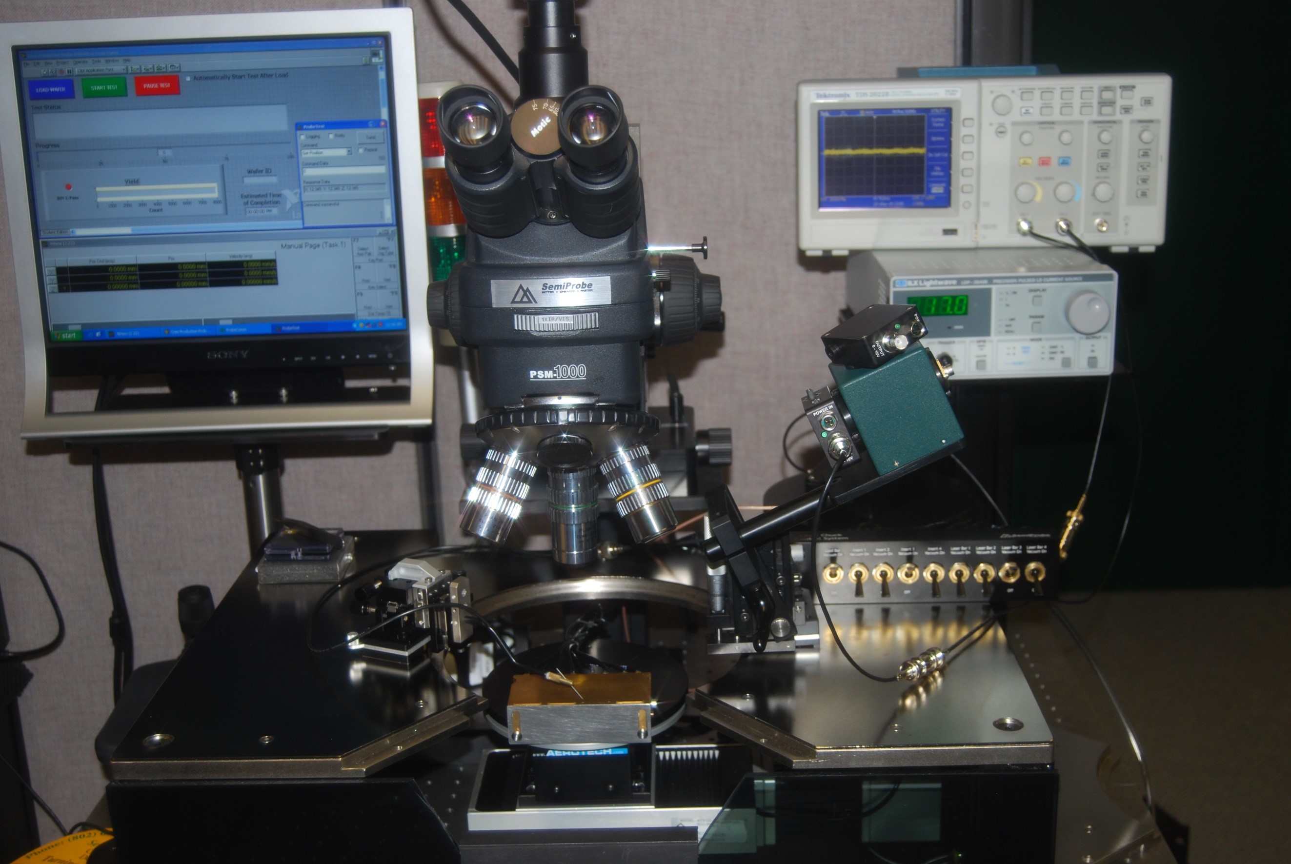
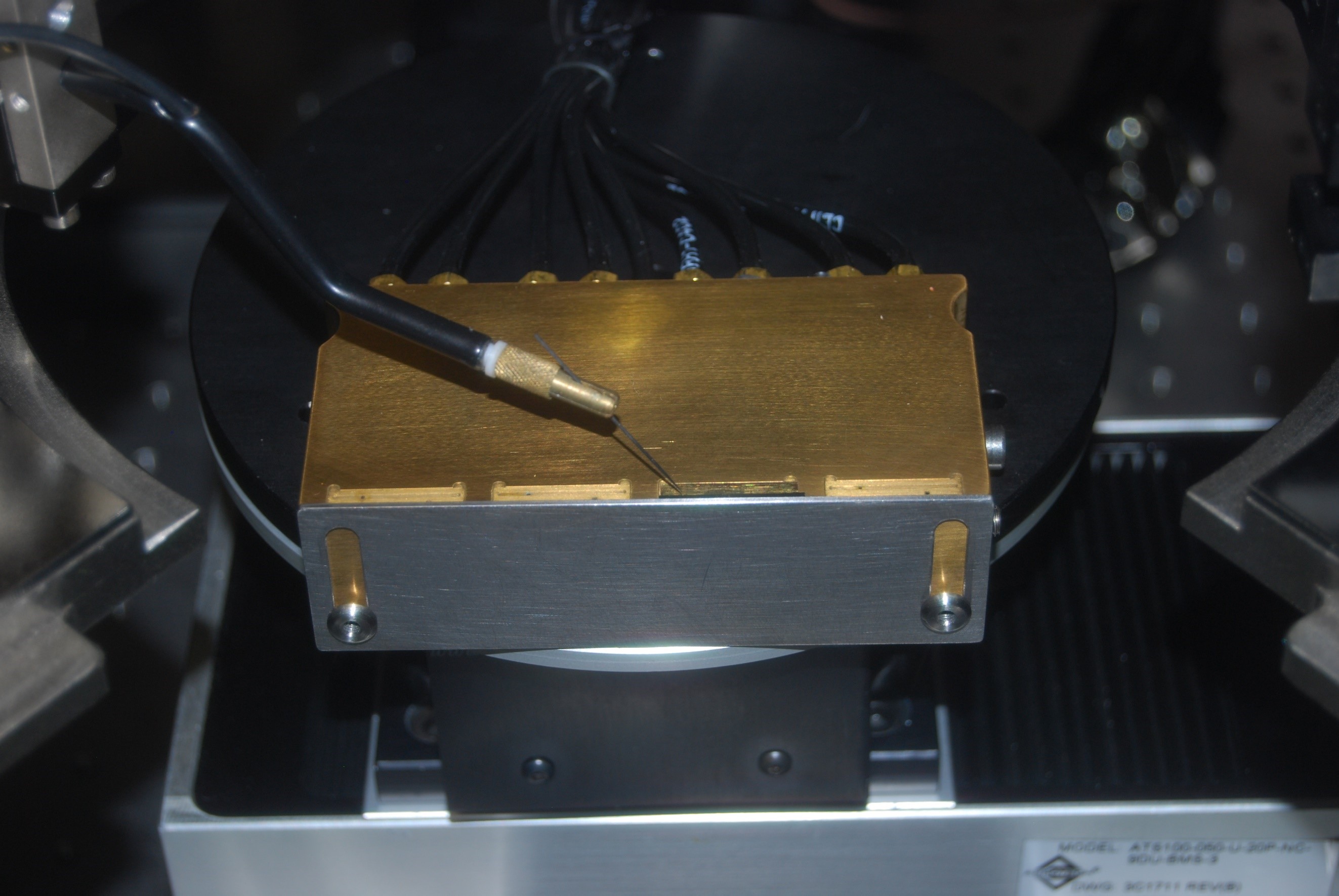
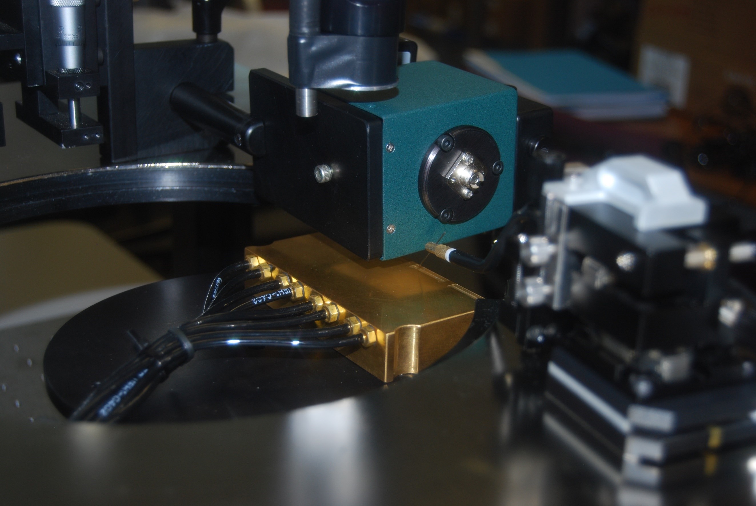
The customer wanted a multipurpose semiautomatic probe system to test vertical-cavity surface-emitting laser diodes (VCSELS) and edge-emitting laser diodes (EELDS) on the same system using a single integrating sphere. The VCSELS would be in wafer form and the EELDS would be in laser bars.
Using our patented Probe System for Life (PS4L) Adaptive Architecture we configured a solution consisting of:
- SA-6 Semiautomatic Probe System
- 150 mm programmable X,Y,Z and theta stage
- PILOT Software Suite – Navigator, Wafer Map and Autoalign
- Vibration Isolation Table
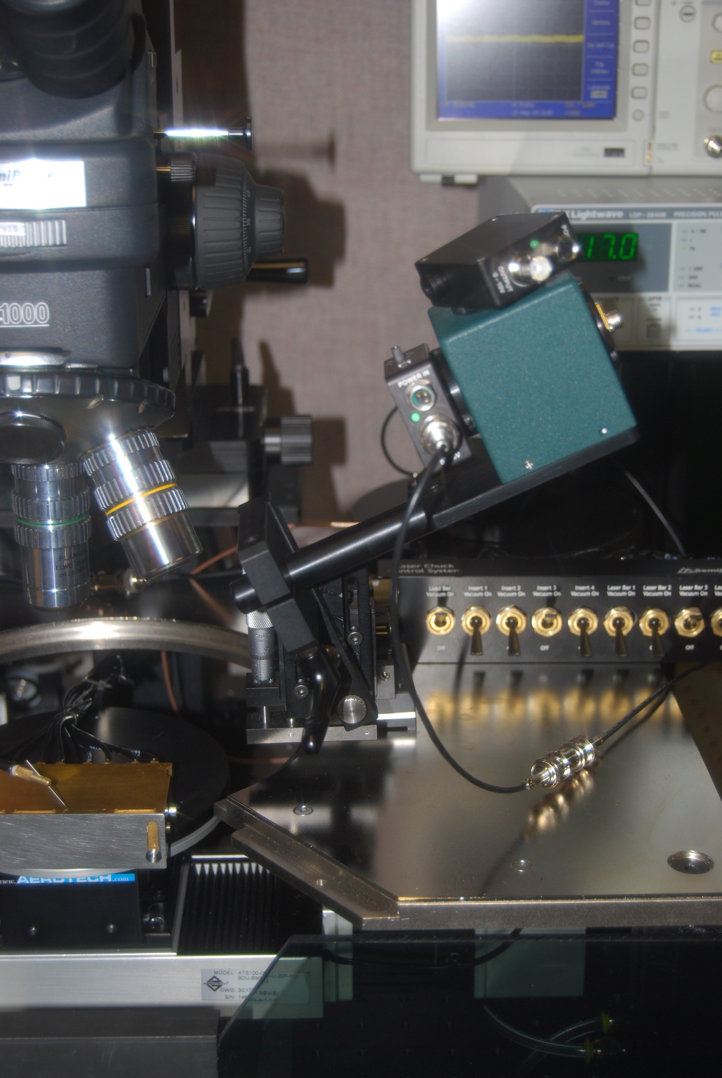
- Multi-Purpose gold plated chuck that allowed both VCSELS and EELDS to be mounted and held via vacuum
- Individual vacuum fixation for the EELD devices/bars
- Single Integrating Sphere used for both applications
- Minimum changeover required to address both requirements – VCSELS and EELDS
- Compound Optics with CCTV System
- Manual Manipulators with coaxial probe arms and DC probe tips
To learn about more advanced Optoelectronic Wafer Probers Click Here