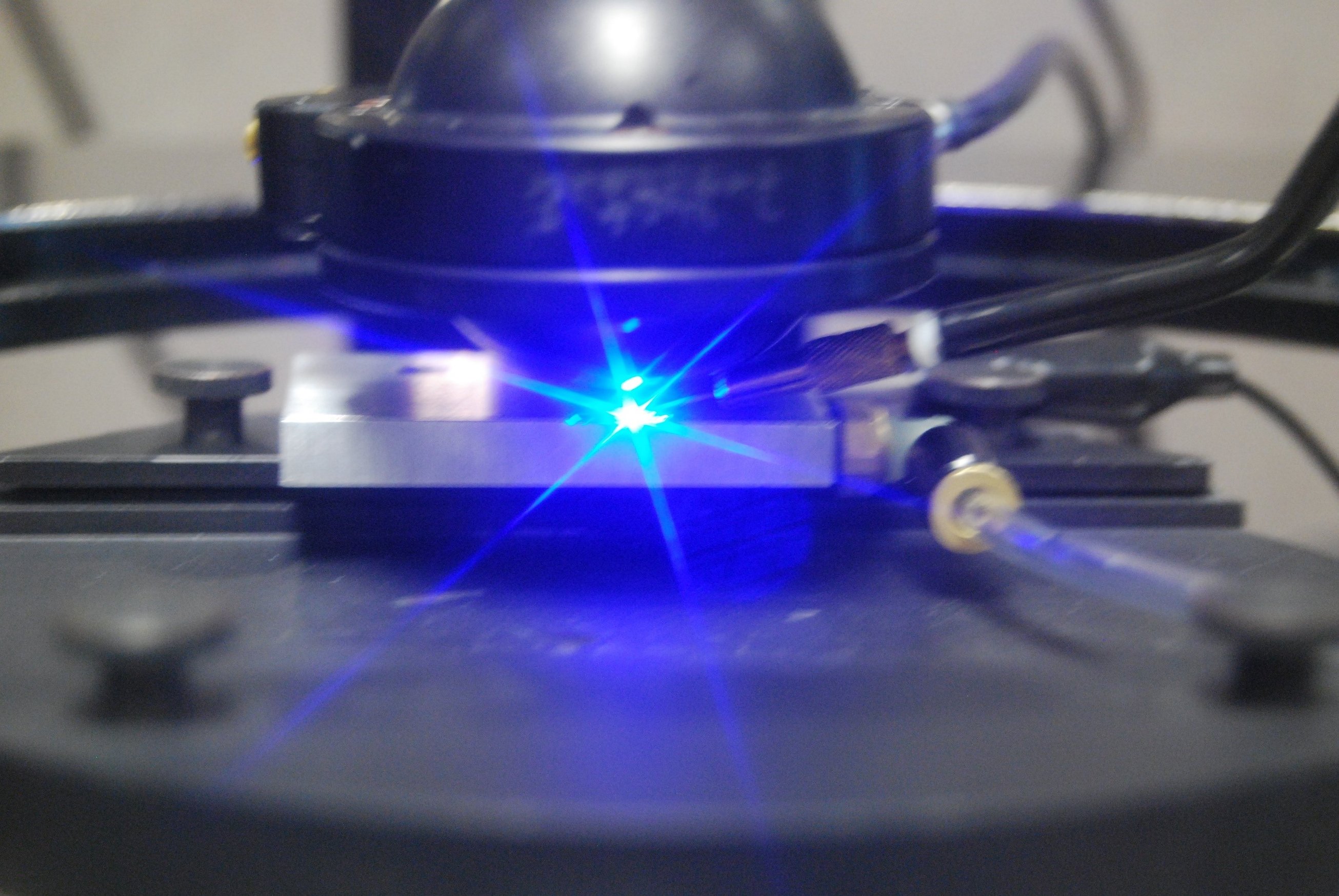
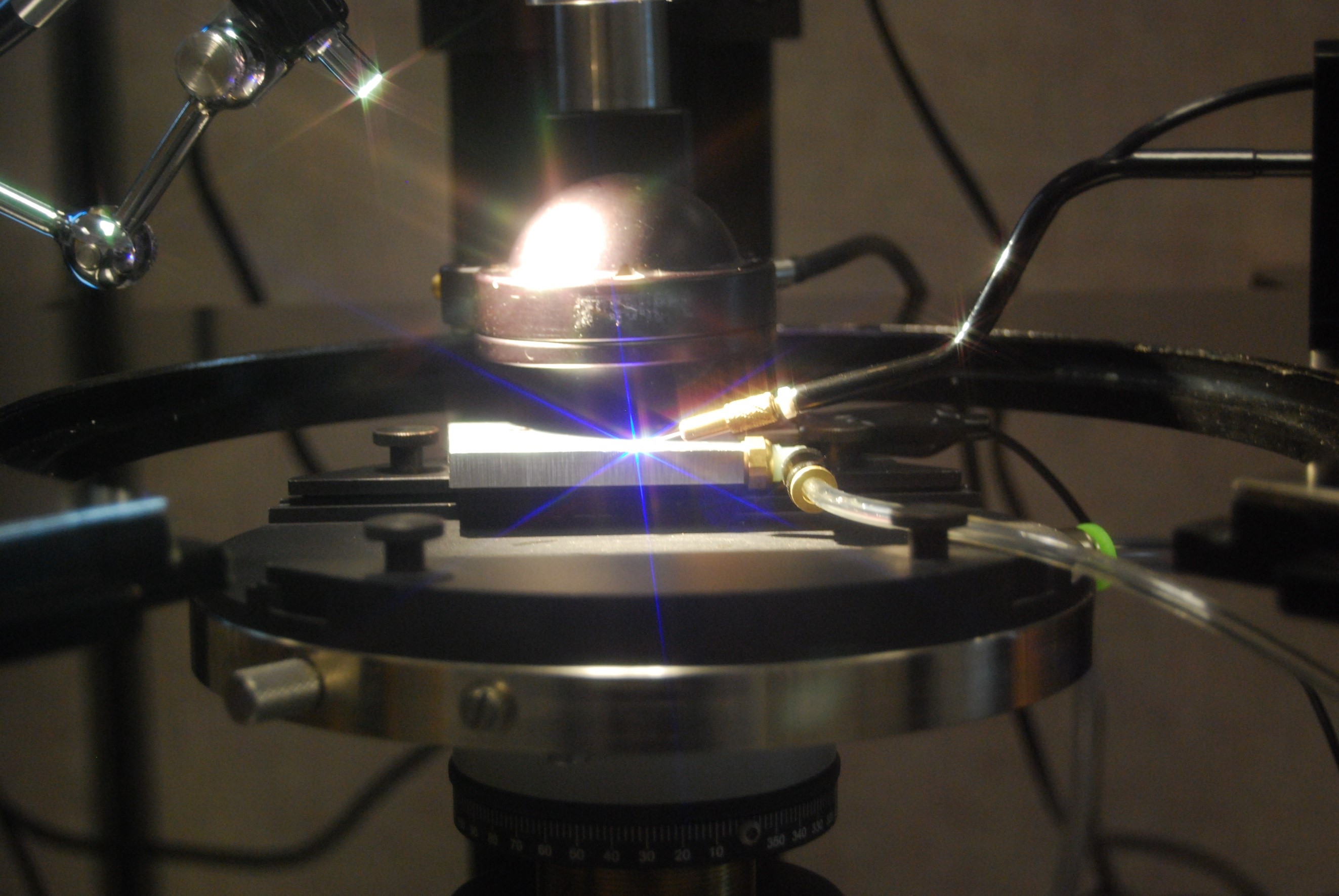
The customer wanted a semiautomatic probe system to test light emitting diodes (LEDS) in a few different modes - wafer form, wafers sawn and stretched on frames or rings, as partial wafers and as individual die. The device would be biased with a DC manipulator and the light output would be captured by an integrating sphere. The integrating sphere needed to be moved in and out of position on a repeatable basis when required.
LED Wafer Prober with Integrating Sphere
Light Emitting Diodes (LEDS)
- SA-6 Semiautomatic Probe System
- 150 mm programmable X,Y,Z and theta stage
- PILOT Software Suite – Navigator, Wafer Map and Autoalign
- Vibration Isolation Table
- Standard (non-thermal) 150 mm wafer chuck and customized holders for frames, rings and die
- Ability to test whole wafers, partial wafers, individual die and wafers sawn & stretched on rings or frames
- Integrating Sphere mounted on a manually moved retractable stage
- Manual Manipulator with coaxial probe arm and DC probe tip
LED Testing with Integrating Sphere
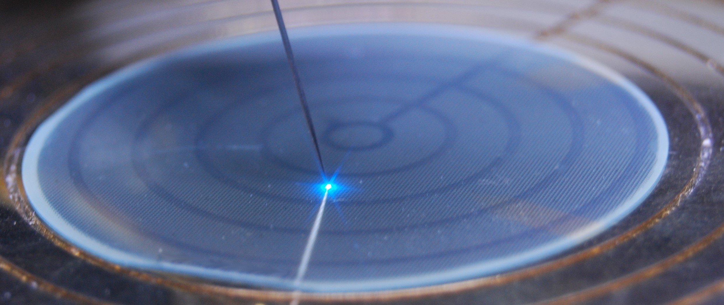
LED Wafer Under Test
To learn more about Advanced Optoelectronic Wafer Probers Click Here