Customer Requirements:
A customer wanted to automatically test individual filters used for 5G applications. The requirement was for a fully automatic RF probe station used in a high-volume wafer production environment that operated 24/7. The RF devices were not in wafer form and could have variations in X,Y,Z and theta from device to device. The customer wanted to use a customized common carrier that would be used pre and post probe.
There was a family of devices to test at High Frequency (RF) so one of the manipulators was manual (3 axis) and the other was programmable (3 axis). This allowed one RF probe to remain fixed in contact while the other RF probe could be moved to contact various sized devices.
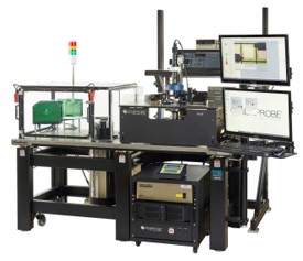
Fully Automated RF Probe Station
SemiProbe RF Probe Station Solution:
- PS4L FA-8 (200 mm) wafer RF probe station consisting of:
- 205 mm x 205 mm programmable X,Y,Z and theta stage and control electronics
- 200 mm High Frequency (RF) chuck with lift pins and two (2) independent calibration substrates
- Non-Contact height measurement system
- Microscope bridge and microscope movement (100 mm x 100 mm) with locking axis knobs
- Compound Optics with motorized focus, customized lighting and CCTV system
- PC/Monitors/Keyboard/Mouse with Adjustable Racks (monitor and test instrumentation)
- PILOT Software Suite – Navigator, Wafer Map and Autoalign
- A material handling unit (MHU) with end-effector, scanner, pre-aligner, bar code reader and safety enclosure with interlocks
- Manual and Programmable High Frequency (RF) manipulators, RF probe arms, RF probes, calibration substrates, RF cables, DC manipulator, probe tips and Inker
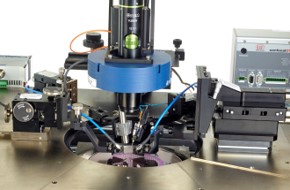
RF Probe Station Closeup
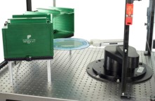
RF Probe Station - Frame Handling System
To learn about our range of advanced Wafer Probe Testing systems go here.