Customer Requirements:
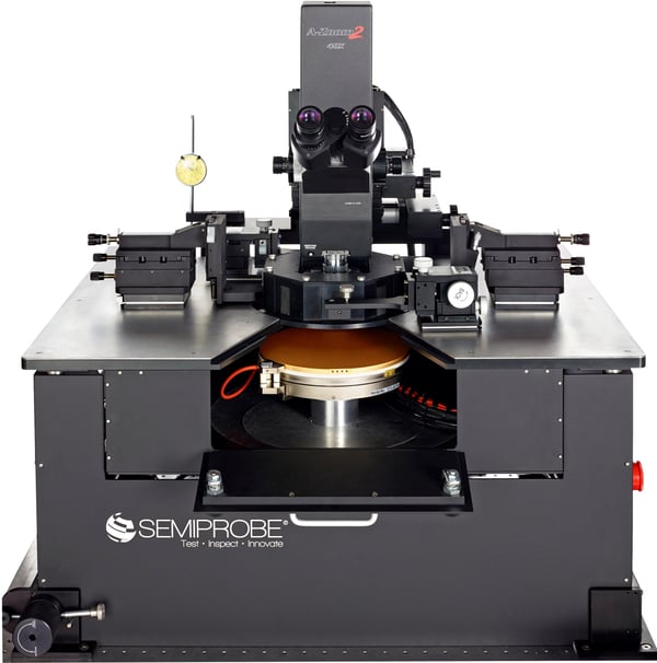
- The customer required a semiautomatic 200 mm probe system that would be used to probe a variety of rf (HF) devices up to 40 GHz. Wafer material could be either silicon or III-V compound. The system had to provide temperature capabilities that ranged from -60 C to 200 C. The devices would get contacted with rf probe cards, multi-contact wedges, rf probes and DC needles. Eight (8) manual manipulators were required – 4 HF and 4 DC with appropriate rf probe arms, rf probe tips and cables.
SemiProbe Solution:
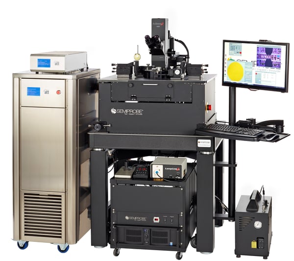
- A PS4L SA-8 (200 mm) semiautomatic rf probe system
- 200 mm programmable X,Y,Z and theta stage with 200 mm load stroke and control electronics
- A 200 mm gold plated thermal chuck with vacuum holes and two (auxiliary chucks) that operated from -60 C to 200 C
- A localized environmental chamber (LEC) with a top hat to provide frost-free, dark and EMI shielding
- Vibration Isolation Table (VIT)
- Compound Microscope Bridge with Compound Microscope Movement (50 mm of X and Y) and 50 mm of pneumatic Z
- Compound Optics and CCTV System
- PC/Monitors/Keyboard and Adjustable Rack
- PILOT Software Suite – Navigator, Wafer Map and Autoalign
- Eight (8) manual manipulators – 4 HF and 4 DC with HF and DC probe arms
- DC and RF probes and calibration substrates
- Air Compressor and Vacuum Pump