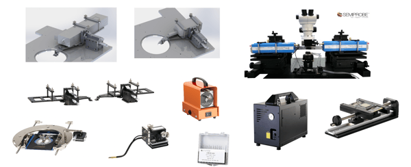
As a manufacturer of wafer probe systems, we are often asked if we manufacture RF Wafer Probes, High Frequency Wafer Probes, Microwave Wafer Probes or mm Wave Wafer Probes. The answer is yes to all but in reality, there is very little difference in how we manufacture a probe system to meet all of the frequency bands mentioned above and below.
While all of these terms are used, the most common term for a high frequency wafer probe system is RF Wafer Probe. We design our RF Wafer Probe systems to meet the customers application and budget. When required the customer can add new modules and accessories in the field to address their new requirements (see PS4L – Wafer Probe Testing System for Life). The application will indicate the frequency the RF Wafer Probe will get configured to meet.
From a SemiProbe standpoint as long as there are probes, cables, calibration substrates and test instrumentation available it’s technically immaterial what frequency you want to test at. We manufacture a line of manual, semiautomatic and fully automatic wafer probe systems with a complete line of modules and accessories to support a variety of RF frequencies and bands.
We integrate all the components mentioned to provide an application specific RF Wafer Probe or a turn- key RF Wafer Probe solution.
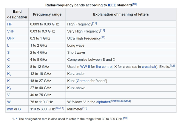
IEEE RF Bands
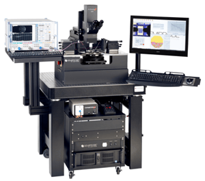 Frequency bands in the microwave range are designated by letters. Microwave (RF) signals are often divided into three (3) categories – ultra high frequency (UHF), super high frequency (SHF) and extremely high frequency (EHF). UHF operates from (0.3 to 3 GHz), SHF operates from (3 GHz to 30 GHz) and EHF operates from (30 GHz to 300 GHz). Most RF Wafer Probe systems are configured to test in the microwave range (0.3 GHz to 300 GHz). This convention began around World War 2 with military designations for frequencies used in radar, which was the first application of microwaves.
Unfortunately, there are several incompatible naming systems for microwave bands around the world and even within a given system the exact frequency range designated by a letter may vary somewhat between different application areas. One widely used standard is the IEEE radar bands established by the US Institute of Electrical and Electronics Engineers.
Note: The Radar Frequency (RF) Band Chart was obtained from the Wikipedia website
SemiProbe manufactures application specific probing solutions using our patented Probe System for Life (PS4L) Adaptive Architecture. Some of the modules and accessories required for an in integrated RF Wafer Probe or Microwave Wafer Probe solution:
- RF Wafer Probe system bases and mechanics need to be rigid to provide vibration free probing – the same could be said for almost any other probing application
- Sometimes a vibration isolation table (VIT) is required
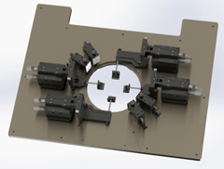
- Platens – hold the manipulators, tuners, extension modules and more. They are typically larger, made of steel or have a steel skin and can also have tapped and drilled mounting holes. In most cases the larger manipulators with mounts for extension modules or tuners are bolted into place due to the cantilevered weights of the instruments.
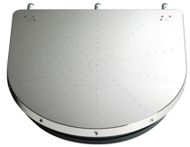
- Wafer Chucks – both standard and thermal chuck top surfaces are manufactured with small vacuum holes to minimize the mechanical stress on III-V materials. Wafer Chucks can be round or square, made from aluminum or steel and have nickel or gold plating.
- Calibration Substrate Holders – used on both standard and thermal chucks. Two (2) are normally provided and the substrates are held in place with independent vacuum lines (wafer chuck and calibration substrate holders have independent vacuum lines).
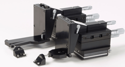
- Manipulators – doe to the additional weights of the cables and probes (GS,SG, GSG, Differential and multi-contact wedges), tuners and extension modules, the manipulators have to be rigid and offered with both magnetic and bolt down bases.
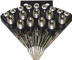
- RF Probes & RF Probe Cards – SemiProbe does not manufacture them because there are a number of companies that already do – GGB Industries, Formfactor (Cascade), Rosenberger, MPI and more. They also manufacture calibration substrates. The customer selects the probes and calibration substrates they want to use and we integrate them to be used on our probe systems.
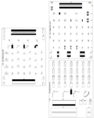

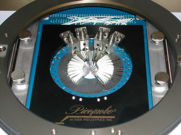
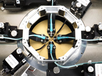
- RF Probe Cables – Several worldwide manufacturers and types. Cables manufactured by Junkosha, Gore Mega-Phase and more are often used. We just need to know what frequency you want to test at and will either use what the customer is already using or include them with the probe system.
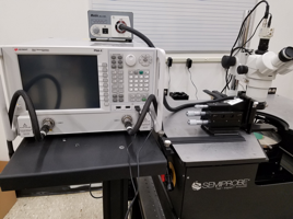
- RF Test Probe Instrumentation – the customer typically has or will purchase the test instrumentation directly from the manufacturer. There are several worldwide suppliers of test instruments such as Vector Network Analyzers – Keysight, Anritsu, Rohde & Schwarz, Copper Mountain, National Instruments, etc. We just have to make sure we can interface to them.
- RF Tuners – usually manufactured by Focus Microwaves or Maury Microwave. SemiProbe just has to make sure we have mechanical mounts for the wide assortment of tuners offered.
- RF Test Probe Instrumentation Racks – SemiProbe has developed a family of test instrumentation racks that are adjustable and designed to allow easy access to the test instrumentation while keeping cable lengths to a minimum.

Common Accessories used to configure application specific RF/Microwave probing solutions:
