Success Story – Europe
Optoelectronic Probe System with Thorlabs Multi-Axis Programmable Manipulators
Customer Requirements:
- Manual Double Sided Probing System (DSP) for testing optoelectronic devices in die and module form.
- Manual loading and un-loading of the device
- The system had to be configured to electrically stimulate from the top of the device and optically stimulate and detect from the side of the device.
- The manual three axis manipulators were placed on the top platen.
- The programmable multi-axis optical manipulators were located underneath the top platen and placed on the bottom side platen.
- The devices were heated and cooled with a thermal electric cooler (TEC).
- DC and HF Probes are used.
SemiProbe Solution:

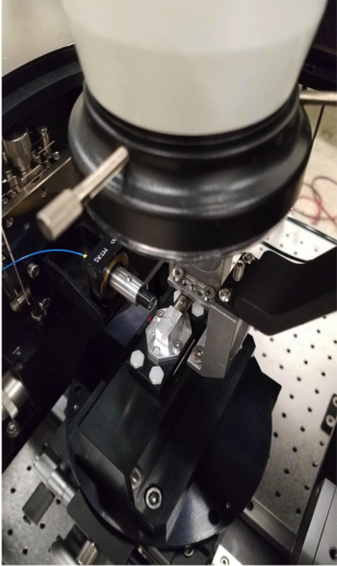
Top Vier of DUT holder and fiber

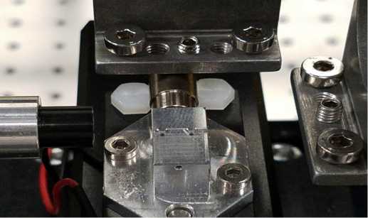
DUT holder with fiber and HF probe mounts

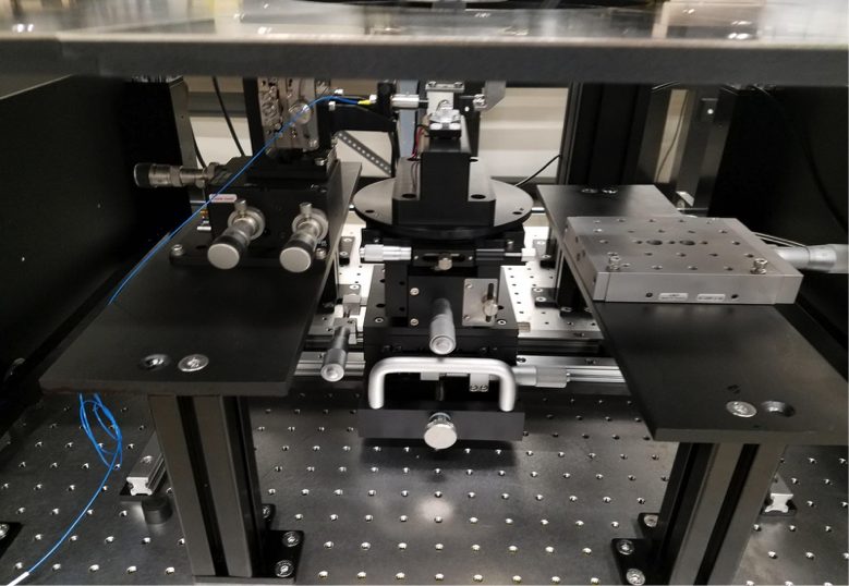
Programmable Manipulator with fiber mounted on bottom platen.
Key System Components:
- Probe System for Life (PS4L) M-4 manual probe system with Rapid Align wafer stage that includes coarse and fine X, Y, Z and theta.
- Double Sided Prober (DSP) platen assembly to support two (2) programmable Thorlabs manipulators and three (3) manual manipulators with customized High Frequency probe arms
- Manual microscope with zoom tube optics with a CCTV System
- Customized TEC thermal system with integrated thermocouples for temperature feedback
- Customized device holder
To learn more about Advanced Optoelectronic Wafer Probers Click Here.


