Success Story – MEMS – United States
Customer Requirements:
- Fully Automatic vacuum probing system for high volume testing of MEMS wafers
- The system had to handle 100 mm and 150 mm wafers automatically and operate in a vacuum environment to 15x10-3 Torr
- DC and High Frequency probe tips and a vacuum compatible high pin probe card with up to 100 SMA connections
- Wafers are standard silicon and or silicon with EPI layers
- Die size ranged from 3 mm to 9 mm in size and Bond Pads ranged from 2 mil to 4 mil
SemiProbe Solution:
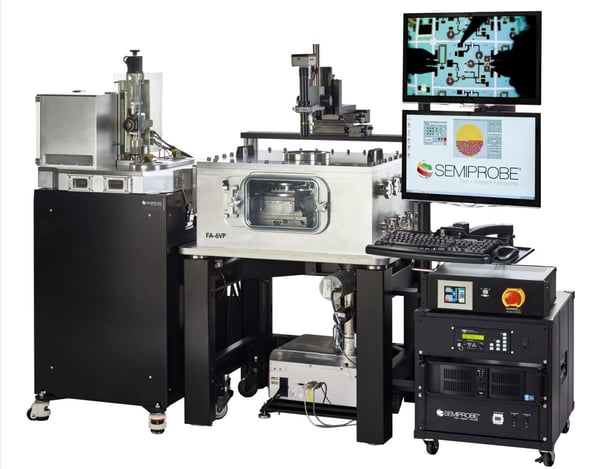
Fully Automated Vacuum Prober for MEMS Testing
Key System Components:
- Vibration Isolation Table (VIT)
- Vacuum Chamber with side and front-loading wafer capabilities and removable top
- 150 mm wafer stage with programmable X, Y, Z and theta stage
- Ambient chuck with mechanical wafer clamping
- Material Handling Unit (MHU) – single cassette (100 mm & 150 mm) with end effector, pre-aligner and load lock
- Large travel microscope movement with Zoom Tube optics and CCTV System
- Three (3) programmable three (3) axis manipulators with customized probe arms – DC & HF
- Probe Card Holder (PCH)
- Software – PILOT Suite (Pilot, Wafer Map, Auto-Align and MHU)
- Turbo Molecular Vacuum Pump with Dual Channel Throttle Valve Controller
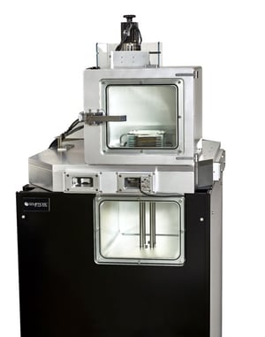
Material Handling Unit (MHU) with Cassette and Load Lock
System Summary:
The probe system can be operated in semiautomatic and fully automatic modes. It can be controlled locally or remotely.
To learn about more advanced MEMS Wafer Probers Click Here