Success Story - USA
When a major University research center called for the unique ability to hold and control a magnetic source within 2 mm of the bottom of their device under test (DUT), they utilized the flexibility of the Probe System for Life (PS4L) universal test platform to create a unique system and do so under severe budget constraints.
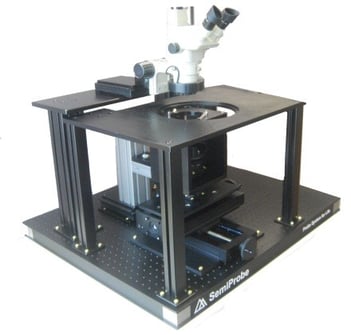
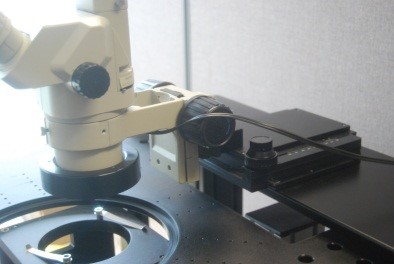
Manual Magnetic Stimulation Wafer Probe Station
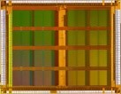
Ferroelectric Random Access Memory (FeRAM or FRAM), Magnetoresistive Random Access Memory (MRAM), and Spintronics research projects share in their use of ferromagnetic materials to control the “switching” of a transistor. The primary advantage seen in these technologies is the non-volatile characteristics of the device. The potential to create a disruptive technology is driving researchers to explore each avenue to determine which method best creates a “new” memory device for computers that is faster and allows users immediate access to data that is stored for long periods of time with no power consumption.
SemiProbe utilized Probe Station for Life (PS4L) standard components in this system and created new capabilities for holding a small wafer or fragment on a thin glass chuck Underneath the DUT. A powerful magnetic source was mounted so that it could be controlled in X, Y, Z, and theta. While doing so, the wafer could be moved in a traditional manner to test multiple devices on the wafer or fragment. Individual probes were used to make device contact. Because the chuck is transparent, the StereoZoom microscope could be used to align the starting position of the magnet.
DUT
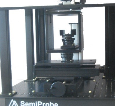
X, Y Z Theta Stage with Magnet Holder
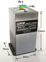
Chucks for several different wafer sizes were fabricated. The chucks are easily exchanged and include a planarization feature for precision planarization to the magnet just below. With the GMW magnetic source held 2 mm below the device, accurate planarity adjustment is imperative.