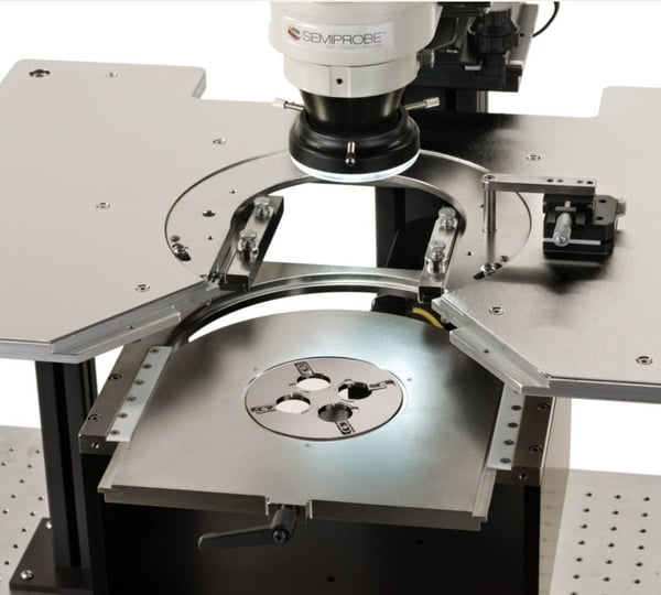
The customer wanted a manual double-sided probing (DSP) system to test silicon photonic chips and wafers using probe cards and manipulators. The top side of the device would be biased and the backside of the device had a light output that was captured by a detector. The detector was mounted on a manual X,Y, Z and theta stage. The devices tested had a variety of dimensions so a universal mechanically clamping chip carrier was designed to hold the devices. Carriers for different size wafers were also required
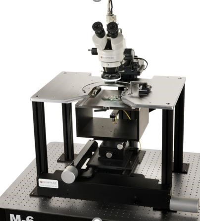 Manual 150 mm Probe System
- 150 mm manual X,Y,Z and theta stage
- Vibration Isolation Table
- Yoke Assembly with individual and removable carriers for wafers and individual die
- Probe Card Holder (PCH) with coarse and fine theta adjust
- Manipulators with DC probe arms, cables and probe tips
- Optical Detector mounted to a manual manipulator with X,Y,Z and theta movement
- Stereozoom Optics with CCTV System
To learn more about other Advanced Optoelectronic Wafer Test Systems Click Here.


Topics:
Application - Optoelectronics,
Application - Double-Sided,
Success Stories,
Manual Systems
Denis Place is one of the founders of SemiProbe and has more than 35 years of experience working in the international semiconductor industry. He has degrees in electrical engineering and business management. Place is in a unique position, because he personally used and worked with probing systems for many years before starting his own semiconductor probing company.

