The customer wanted a 300 mm fully automatic double-sided probe system for high volume silicon photonics testing in a production environment. The system had to provide the ability to bias the device with a probe card on the top while detecting light output from the bottom of the wafer. The system needed to provide low and high temperature capability from -40 C to 200 C in a frost-free and shielded environment. The system had to be able to operate 24 hours a day, 7 days a week. The system had to be tested to and certified to a variety of SEMI, UL and other safety standards.
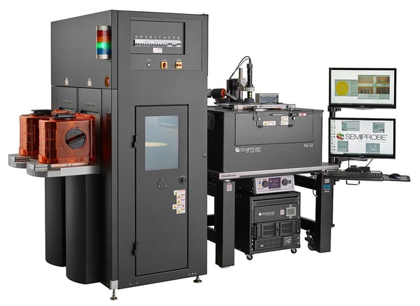
- A PS4L FA-12 (300 mm) probe system consisting of:
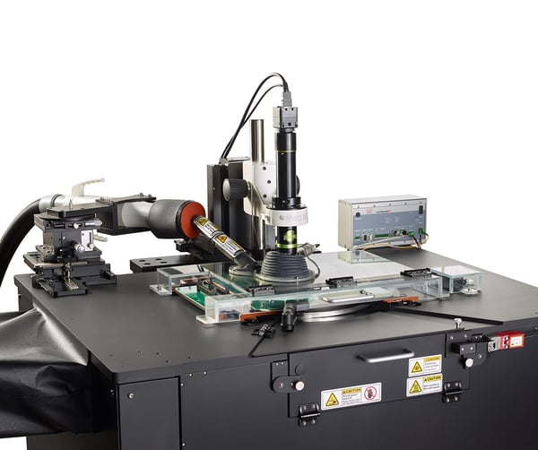
- 305 mm x 305 mm programmable X,Y,Z and theta stage
- A double-sided 300 mm wafer carrier assembly
- A localized environmental chamber (LEC) and cover
- A programmable coarse and fine X,Y,Z stage with mount for backside detector
- A compound microscope bridge and microscope movement (100 mm x 100 mm) with a pneumatic 50 mm Z lift
- Compound Optics and CCTV System
- PC/Monitors/Keyboard/Adjustable Rack
- PILOT Software Suite – Navigator, Wafer Map and Autoalign
- A non-contact height measurement system
- A thermal system that can operate from -40 C to 200 C
- A material handling unit (MHU) that can handle two (2) 300 mm FOUPS with AGV loading and un-loading
- Fully Certified SEMI System
To learn more about other Advanced Optoelectronic Wafer Probers Click Here.