Customer Requirements:
- Semiautomatic 300 mm Double Sided Probing (DSP) System to characterize several different types and sizes of silicon photonic devices in a shielded environment. The system had to test 150 mm, 200 mm and 300 mm wafers and individual die.
SemiProbe Solution:
- 300 mm Semiautomatic DSP Optoelectronic Device Characterization System with programmable X, Y, Z and theta movement and control electronics
- Localized Environmental Chamber (LEC) with Top Hat to provide dark and EMI shielded environment
- Customized vibration isolation table (VIT)
- Large travel gantry to accommodate a few different types of optics and instruments. Independently controlled X, Y, and Z movements – manual and programmable
- Manual manipulators for topside and bottom side probing and a probe card holder
- Non-Contact Height Measurement Sensor
- Topside and bottom-side optics and cameras
- Universal carrier plate to hold different sized die, partial wafers and whole wafers up to 300 mm
- Detector mounted on a small travel programmable stage for optimization of output light collection
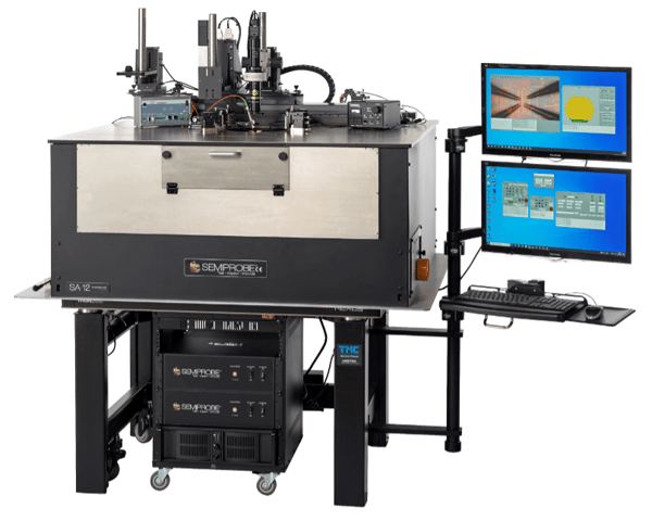
SemiProbe PS4L SA-12 Semiautomatic Double-Sided Probing Optoelectronic Device Characterization System - configured to test silicon photonic wafers and die
%20to%20provide%20EMI%20and%20Light%20shielding.%20%20A%20large%20optics%20gantry%20to%20hold%20multiple%20optical%20devices.png?width=600&height=533&name=PS4L%20SA-12%20Semiautomatic%20DSP%20Optoelectronic%20Device%20Characterization%20System%20with%20a%20localized%20environmental%20chamber%20(LEC)%20to%20provide%20EMI%20and%20Light%20shielding.%20%20A%20large%20optics%20gantry%20to%20hold%20multiple%20optical%20devices.png)
PS4L SA-12 Semiautomatic DSP Optoelectronic Device Characterization System with a localized environmental chamber (LEC) to provide EMI and Light shielding. A large optics gantry to hold multiple optical devices
%20Optoelectronic%20Device%20Characterization%20System%20for%20testing%20200%20mm%20and%20300%20mm%20silicon%20photonic%20wafer.png?width=600&height=668&name=PS4L%20SA-12%20Semiautomatic%20Double-Sided%20Probing%20(DSP)%20Optoelectronic%20Device%20Characterization%20System%20for%20testing%20200%20mm%20and%20300%20mm%20silicon%20photonic%20wafer.png)
PS4L SA-12 Semiautomatic Double-Sided Probing (DSP) Optoelectronic Device Characterization System for testing 200 mm and 300 mm silicon photonic wafer
%20Optoelectronic%20Device%20Characterization%20System%20with%20top%20and%20bottom%20platens%20and%20manipulators.png?width=600&height=604&name=PS4L%20SA-12%20Semiautomatic%20Double-Sided%20Probing%20(DSP)%20Optoelectronic%20Device%20Characterization%20System%20with%20top%20and%20bottom%20platens%20and%20manipulators.png)
PS4L SA-12 Semiautomatic Double-Sided Probing (DSP) Optoelectronic Device Characterization System with top and bottom platens and manipulators