Success Story - USA
When a leading innovator of integrated circuits, hybrids and modules used in industrial and aerospace applications that require high-power precision analog products, such as PWM and power amplifiers needed to apply semiconductor device characterization to their devices, they turned to the Probe System for Life (PS4L).
These precision amplifiers are used for driving motors, piezo electrics, programmable power supplies and other semiconductor devices requiring high power and precision control.
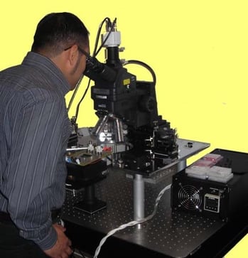
Manual PS4L Probe System with Compound Optics and Thermal Control System for Semiconductor Device Characterization
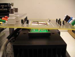
This semiconductor device characterization application required the ability to quickly change configurations from ambient to high temperature and the ability to probe semiconductor devices mounted on printed circuit boards (PCB).
For the semiconductor Failure Analysis (FA) application, one form of device characterization, high power magnification was needed to land probes on small structures. For this reason, a compound microscope was chosen. Probing on these small structures for semiconductor device characterization also required vibration isolation because the base of the PS4L system is integral to the vibration isolation system, the machine base became the table top for the isolation system. The devices to characterize were small and required a minimum of stage travel.
For this reason, the PS4L offered an advantage of a small but precise stage with micrometer drives for positioning. Within minutes, this small stage could be removed and replaced with the thermal unit custom configured to hold the device board at elevated temperature. The semiconductor device was then characterized using the same components used on the standard stage. The unique small thermal unit for packaged parts, small semiconductor wafers and fragments provided the customer with a significant cost advantage over using the thermal chuck solutions offered by competitors. 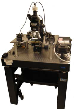
Versatile PS4L Manual Probing Platform used to Characterize Semiconductor Wafers, Devices and Packaged Parts
The PS4L probing semiconductor device characterization platform was designed to provide the customer many options on how to configure their system. All key building blocks are interchangeable. There are numerous accessories and modules that can be purchased initially or at a later date.
To learn more about our complete Wafer Probe Testing Solutions go here.