Customer Requirements:
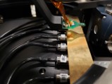
The customer wanted a semiautomatic wafer probe testing system to test high power edge emitting laser diodes (EELD) in laser bar form. There were several EELDS per laser bar and a family of different sized bars that needed to be tested and held in place. They needed a customized fixture that allowed them to load and unload the laser bars from outside the wafer probe testing system.
Every laser bar had independent vacuum fixation and there were multiple laser bars mounted on a fixture. The fixture had to be designed to allow easy loading and un-loading of the fixture. Every EELD would need to be tested and the system had to compensate for slight variations in X,Y,Z and theta from bar to bar. The device would be stimulated from the top with a customized probe assembly. Light output was collected by an integrating sphere. A customized graphical user interface (GUI) had to control the prober and test instrumentation as well as collect the data for analysis.
.jpg?width=200&name=Picture16%20(2).jpg)
SemiProbe Solution:
Edge-Emitting Laser Diodes in bar form
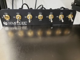
- Semiautomatic 150 mm Probe System
- 150 mm programmable X,Y,Z and theta stage with control electronics
- PILOT Software Suite – Navigator, Wafer Map and Autoalign
- Customized Graphical User Interface (GUI)
- Top side probing with manipulators and customized probe assembly
- Customized EELD laser bar carrier with individual vacuum
- Integrating sphere with customized mount
- Two types of optics for topside and sideward device and probe alignment
- Vibration Isolation Table with adjustable monitor, keyboard and mouse rack