Customer Requirements:
The customer wanted a wafer probe testing solution to test a variety of wafers ranging in size from 100 mm to 200 mm at high voltages in a vacuum environment. They wanted the ability to test both vertical and lateral devices at ambient and up to 10 KV. They wanted the ability to use probe cards as well as individual programmable manipulators with HV and DC probe arms. The probe system would need the ability to interface to a Keysight B1505 parametric analyzer and other test instrumentation.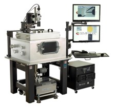
SemiProbe Wafer Probe Testing Solution:
Semiautomatic 200 mm Vacuum Wafer Probe Testing System
- SA-8 Semiautomatic 200 mm Wafer Probe System
- 200 mm programmable X,Y,Z and theta stage with control electronics
- PILOT Software Suite – Navigator, Wafer Map, Autoalign and Programmable Manipulator Modules
- Vibration Isolation Table
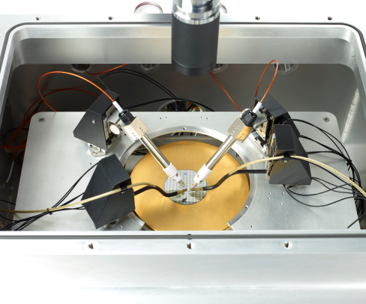
- Large Vacuum Chamber with removable top and front- loading door for easy loading and unloading of devices
- Triaxial Chuck System that operates at ambient
- All Components in the vacuum chamber rated to 10-5 torr
- Agilent turbo-molecular vacuum pump
- Large microscope bridge and movement with X,Y Z and theta for long working distance optics with a motorized focus
- Compound Optics with CCTV System
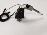
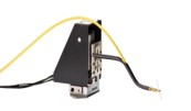
- Programmable Manipulators and Probe Cards
- Four (4) programmable three axis manipulators with coaxial HV (10 KV) and low voltage (600 V) triaxial DC probe arms, cables and probes
- Probe Card Holder – 4.5” cards
- Integrated with Keysight B1505 Parametric Analyzer