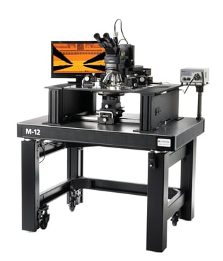
What’s the difference between a wafer prober and a Probe Station for Life (PS4L)?
A wafer prober, otherwise known as a semiconductor probe station, or probe station, are tools used for testing circuits and devices on silicon wafers, dies and open microchips. The Probe System for Life (PS4L) is a type of wafer prober, but it has many benefits and capabilities that other wafer probers do not offer.
- What are probe stations used for?
Wafer Prober stations enable users to position electrical, optical or RF probes on a silicon wafer to examine the device under test (DUT). These tests can be simple, such as continuity or isolation check, or sophisticated, including full functional testing of microcircuits. Tests can be run either before or after the wafer has been sawn into individual dies.
By testing at the wafer level with a wafer prober, manufacturers can test a device multiple times throughout the production process. This helps provide insight as to which process steps are creating defects into the finished product. It also enables manufacturers to test the dies prior to packaging, which is important in applications where the packaging costs are high relative to the device costs.
Finally, wafer probers are often used in R&D, product development and failure analysis applications, where engineers need a flexible, precise tool to conduct tests on different areas on a device.
- What makes the Probe Station for Life (PS4L) different from other wafer probers?
The Probe System for Life, or PS4L, is SemiProbe’s patented adaptive wafer prober system architecture. Unlike traditional wafer prober systems, all of the basic components of our systems, including the bases, stages, chucks, microscope mounts, and manipulators, are interchangeable, upgrade-able, and configurable. The PS4L Adaptive Architecture ensures an optimal test configuration for each individual customer application.
PS4L systems are available to handle products from 50 mm to 300 mm, and are available in manual, semiautomatic, and fully automatic configurations. A unique advantage of the PS4L system is its ability to be upgraded at any point in its life cycle as your product needs or volume requirements change. As the customer’s business environment or test conditions change, the PS4L can be rapidly reconfigured to meet these new requirements. Changes to wafer size, automation level, or test procedure do not translate into a need for new capital equipment. This substantially reduces the cost of new product development and the time to procure the appropriate test equipment. Reconfigurations are typically performed in the field, at the customer site.
For more information on the PS4L, please request a discovery call and someone from our team will be in touch.


